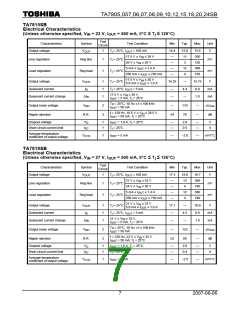
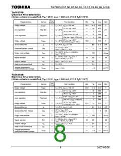
TA7805,057,06,07,08,09,10,12,15,18,20,24SB
Precautions on Application
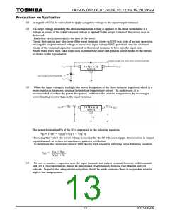
(1) In regard to GND, be careful not to apply a negative voltage to the input/output terminal.
(2) If a surge voltage exceeding the absolute maximum rating is applied to the input terminal or if a
voltage in excess of the input terminal voltage is applied to the output terminal, the circuit may be
destroyed.
Particular care is necessary in the case of the latter.
Circuit destruction may also occur if the input terminal shorts to GND in a state of normal operation,
causing the output terminal voltage to exceed the input voltage (GND potential) and the electrical
charge of the chemical capacitor connected to the output terminal to flow into the input side.
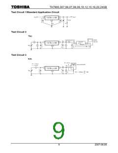
Where these risks exist, take steps such as connecting zener and general silicon diodes to the circuit,
as shown in the figure below.
(3)
When the input voltage is too high, the power dissipation of the three-terminal regulator, which is a
series regulator, increases, causing the junction temperature to rise. In such a case, it is
recommended to reduce the power dissipation, and hence the junction temperature, by inserting a
power-limiting resistor R
in the input terminal.
SD
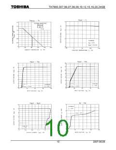
The power dissipation P of the IC is expressed in the following equation.
D
Reducing V
below the lowest voltage necessary for the IC will cause ripple, deterioration in output
IN'
regulation and, in certain circumstances, parasitic oscillation.
To determine the resistance value of R , design with a margin, referring to the following equation.
SD
(4)
Be sure to connect a capacitor near the input terminal and output terminal between both terminals
and GND. The capacitances should be determined experimentally because they depend on PCB
patterns. In particular, adequate investigation should be made to ensure there is no problem even in
high or low temperatures
13
2007-06-06

 TOSHIBA [ TOSHIBA ]