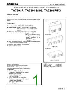
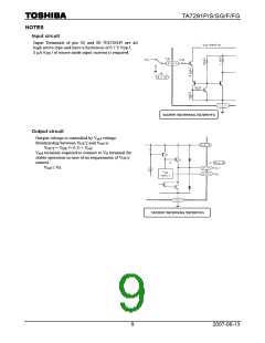
TA7291P/S/SG/F/FG
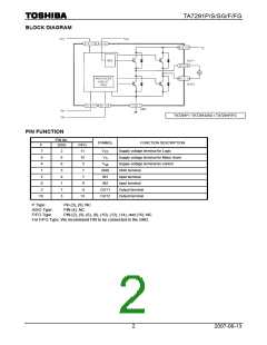
BLOCK DIAGRAM
TA7291P / TA7291S/SG / TA7291F/FG
PIN FUNCTION
PIN No.
SYMBOL
FUNCTION DESCRIPTION
Supply voltage terminal for Logic
P
S/SG
F/FG
11
15
5
7
2
6
8
5
9
1
7
3
V
CC
8
4
V
Supply voltage terminal for Motor driver
Supply voltage terminal for control
GND terminal
S
V
ref
1
1
GND
IN1
5
7
Input terminal
6
9
IN2
Input terminal
2
4
OUT1
OUT2
Output terminal
10
13
Output terminal
P Type:
S/SG Type:
F/FG Type:
Pin (3), (9): NC
PIN (4): NC
PIN (2), (3), (6), (8), (10), (12), (14), and (16): NC
For F/FG Type, We recommend FIN to be connected to the GND.
2
2007-06-13

 TOSHIBA [ TOSHIBA ]