HN1B01F
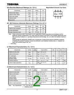
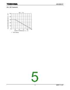
Q2 Absolute Maximum Ratings (Ta = 25°C)
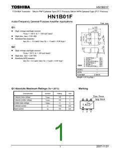
Equivalent Circuit (Top View)
Characteristic
Symbol
Rating
Unit
Collector-base voltage
Collector-emitter voltage
Emitter-base voltage
Collector current
V
V
V
60
50
5
V
V
CBO
CEO
EBO
V
I
150
30
mA
mA
C
Base current
I
B
Q1, Q2 Common Absolute Maximum Ratings (Ta = 25°C)
Characteristic
Symbol
P *
Rating
Unit
Collector power dissipation
Junction temperature
300
125
mW
°C
C
T
j
Storage temperature range
T
stg
−55~125
°C
Note: Using continuously under heavy loads (e.g. the application of high temperature/current/voltage and the
significant change in temperature, etc.) may cause this product to decrease in the reliability significantly even
if the operating conditions (i.e. operating temperature/current/voltage, etc.) are within the absolute maximum
ratings.
Please design the appropriate reliability upon reviewing the Toshiba Semiconductor Reliability Handbook
(“Handling Precautions”/“Derating Concept and Methods”) and individual reliability data (i.e. reliability test
report and estimated failure rate, etc).
*: Total rating
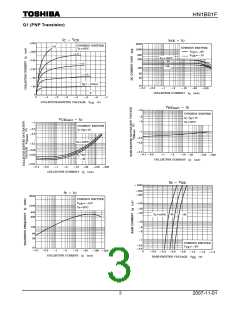
Q1 Electrical Characteristics (Ta = 25°C)
Test
Circuit
Characteristic
Symbol
Test Condition
= −50 V, I = 0
Min
Typ.
Max
Unit
Collector cut-off current
Emitter cut-off current
DC current gain
I
―
V
V
V
―
―
―
―
―
−0.1
−0.1
400
μA
μA
CBO
CB
EB
CE
E
I
―
―
= −5 V, I = 0
C
EBO
h
= −6 V, I = −2 mA
120
FE (Note)
C
Collector-emitter
saturation voltage
V
―
―
―
I
= −100 mA, I = −10 mA
―
―
―
−0.1
120
4
−0.3
―
V
CE (sat)
C
B
Transition frequency
f
V
V
= −10 V, I = −1 mA
MHz
pF
T
CE
CB
C
= −10 V, I = 0,
E
Collector output capacitance
C
―
ob
f = 1 MHz
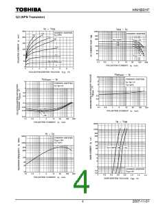
Q2 Electrical Characteristics (Ta = 25°C)
Test
Circuit
Characteristic
Symbol
Test Condition
= 60 V, I = 0
Min
Typ.
Max
Unit
Collector cut-off current
Emitter cut-off current
DC current gain
I
―
―
―
V
V
V
―
―
―
―
―
0.1
0.1
400
μA
μA
CBO
CB
EB
E
I
= 5 V, I = 0
C
EBO
h
= 6 V, I = 2 mA
120
FE (Note)
CE
C
Collector-emitter
saturation voltage
V
―
―
―
I
= 100 mA, I = 10 mA
―
―
―
0.1
150
2
0.25
―
V
CE (sat)
C
B
Transition frequency
f
V
V
= 10 V, I = 1 mA
MHz
pF
T
CE
CB
C
= 10 V, I = 0,
E
Collector output capacitance
C
―
ob
f = 1 MHz
Note: hFE Classification Y (Y): 120~240, GR (G): 200~400
) Marking symbol
(
2
2007-11-01

 TOSHIBA [ TOSHIBA ]