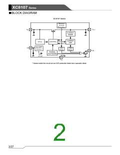
XC8107 Series
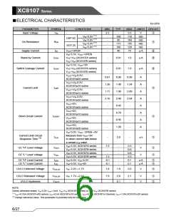
■ELECTRICAL CHARACTERISTICS
Ta=25℃
PARAMETER
Input Voltage
SYMBOL
VIN
CONDITIONS
MIN.
TYP.
MAX.
UNITS CIRCUIT
-
2.5
-
5.5
110
104
135
120
75
V
①
VIN=3.3V (*1)
-
-
-
-
-
100
85
mΩ
mΩ
mΩ
mΩ
μA
USP-6C
VIN=5.0V (*1)
VIN=3.3V (*1)
VIN=5.0V (*1)
On Resistance
RON
①
115
100
40
SOT-25
Supply Current
ISS
VOUT=OPEN
②
②
VIN=5.5V, VOUT=OPEN
Stand-by Current
ISTBY
VCE=VSS (XC8107A series)
VCE=VIN (XC8107B series)
-
-
0.01
0.01
1.0
1.0
μA
μA
VIN=5.5V, VOUT=0V
VCE=VSS (XC8107A series)
VCE=VIN (XC8107B series)
VOUT=VIN-0.3V,
Switch Leakage Current
ILEAK
②
0.81
0.90
1.40
1.90
2.40
0.45
0.70
0.95
1.20
0.99
A
A
A
A
A
A
A
A
XC8107xx05 series
VOUT=VIN-0.3V,
1.26
1.54
XC8107xx10 series
VOUT=VIN-0.3V,
Current Limit
ILIMT
①
1.71
2.09
XC8107xx15 series
VOUT=VIN-0.3V,
2.16
2.64
XC8107xx20 series
VOUT=0V,
-
-
-
-
-
-
-
-
XC8107xx05 series
VOUT=0V,
XC8107xx10 series
VOUT=0V,
Short-Circuit Current
ISHORT
①
①
XC8107xx15 series
VOUT=0V,
XC8107xx20 series
VIN=5.0V, VOUT: OPEN→0V
Measure from VOUT=0V
to when current falls below
a certain ILIM value
VIN=5.5V, XC8107A series
VIN=5.5V, XC8107B series
VIN=5.5V, XC8107A series
VIN=5.5V, XC8107B series
VIN=5.5V, VCE=5.5V
VIN=5.5V, VCE=0V
Current Limit Circuit
Response Time (*2)
tCLR
-
2.0
-
μs
1.5
-
-
-
-
-
-
-
5.5
0.8
0.8
5.5
0.1
0.1
CE "H" Level Voltage
CE "L" Level Voltage
VCEH
VCEL
V
V
①
①
-
1.5
-0.1
-0.1
CE "H" Level Current
CE "L" Level Current
ICEH
ICEL
μA
μA
①
①
UVLO Detected Voltage
VUVLOD
VIN: 2.2V→1.7V
1.8
1.9
2.0
V
①
UVLO Released Voltage
UVLO Hysteresis
VUVLOR
VUHYS
VIN: 1.7V→2.2V
1.9
-
2.0
0.1
2.1
-
V
V
①
①
-
NOTE:
Unless otherwise stated, VIN=5.0V, IOUT=1mA, VCE=VIN (XC8107A series) or VCE=VSS (XC8107B series)
(*1)
I
=0.25A (XC8107xx05 series), IOUT=0.5A (XC8107xx10 series), IOUT=0.75A (XC8107xx15series), IOUT=1.0A (XC8107xx20 series)
OUT
(*2) Design reference value. This parameter is provided only for reference.
6/27

 TOREX [ Torex Semiconductor ]