XC6415
Series
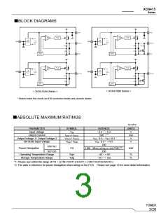
■BLOCK DIAGRAMS
< XC6415BB Series >
< XC6415AA Series >
* Diodes inside the circuits are ESD protection diodes and parasitic diodes.
■ABSOLUTE MAXIMUM RATINGS
Ta=25OC
PARAMETER
Input Voltage
SYMBOL
VIN
RATINGS
UNITS
- 0.3 ~ + 6.5
V
mA
V
(*1)
Output Current
IOUT1 + IOUT2
VOUT1 / VOUT2
VEN1 / VEN2
500
Output Voltage 1 / Output Voltage 2
EN1/EN2 Input Voltage
VSS - 0.3 ~ VIN + 0.3
VSS - 0.3 ~ + 6.5
V
100
1000 (When wiring on the PCB)(*2)
250
USP-6C
Power Dissipation
Pd
mW
SOT-25
Operating Temperature Range
Storage Temperature Range
Topr
Tstg
- 40 ~ + 85
℃
℃
- 55 ~ + 125
*1: Please use within the range of Pd > { (VIN-VOUT1)×IOUT1 + (VIN-VOUT2)×IOUT2 }
*2: The data is reference for power dissipation when wiring on the PCB. Please see page 19 for more detail information.
3/20

 TOREX [ Torex Semiconductor ]