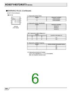
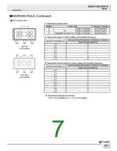
XC6371/6372/6373 Series
■ELECTRICAL CHARACTERISTICS (Continued)
XC6371/72C501PR
VOUT=5.0V, FOSC=100kHz
Ta=25℃
PARAMETER
Output Voltage
Maximum Input Voltage
Operation Start Voltage
SYMBOL
VOUT
VIN
VST1
CONDITIONS
MIN.
4.875
10
TYP.
5.000
-
-
MAX. UNITS
5.125
-
0.90
V
V
V
External Components Connected, IOUT=1mA
No external components. Apply voltage to VOUT,
Lx : 10kΩ pull-up to 5V
-
Operation Start Voltage
No Load Input Current
Supply Current 1
VST2
IIN
-
-
-
-
0.80
25.7
V
VIN=VOUT×0.8, IOUT=0mA (*1)
Same as VST2,
Apply output voltage×0.95 to VOUT
Same as VST2,
12.8
80.2
μA
μA
IDD1
133.8
Supply Current 2
IDD2
-
-
8.2
1.4
16.5
2.4
μA
Apply output voltage×1.1 to VOUT
Lx Switch-On
Resistance
RSWON
Same as IDD1, VLx=0.4V
Ω
Lx Leak Current
ILXL
FOSC
MAXDTY
PFMDTY
ISTB
VCEH
VCEL
No external components, VOUT =VLX=10V
Same as IDD1, Measuring of Lx waveform
Same as IDD1, Measuring of Lx waveform
Same as IDD1, Measuring of Lx waveform
Same as IDD1
-
85
80
10
-
0.75
-
-
1.0
115
92
25
0.5
μA
kHZ
%
%
μA
V
V
μA
μA
Oscillation Frequency
Maximum Duty Ratio
PFM Duty Ratio (*4)
Stand-by Current
CE "High" Voltage
CE "Low" Voltage
CE "High" Current
CE "Low" Current
100
87
17
-
-
-
-
-
Same as IDD1, Lx Oscillation start
Same as IDD1, Lx Oscillation stop
Same as IDD1, VCE=VOUT×0.95
Same as IDD1, VCE=0V
-
0.20
0.25
-0.25
ICEH
ICEL
-
-
Same as IDD1, Apply output voltage to Lx,
Voltage required to produce FOSC×2
Lx Limit Voltage
VLxLMT
0.7
-
1.3
V
Efficiency
Slow-Start Time
EFFI
TSS
-
85
10.0
-
%
ms
4.0
20.0
NOTE: Unless otherwise stated, connect CE to VOUT, VIN=VOUT×0.6, IOUT=50mA. See Typical Application Circuits, Circuit 2.
*1: The Schottky diode (SD) must be type MA735, with reverse current (IR)<1.0μA at reverse voltage (VR)=10.0V.(XC6372C)
*2: "Supply Current 1" is the supply current while the oscillator is continuously oscillating. In actual operation the oscillator periodically
operates which results in less average power consumption. The current actually provided by an external VIN source is represented by
"No Load Input Current (IIN)".
*3: When PWM operates at PWM Mode.
*4: When PFM operates at PFM Mode.(XC6372C)
590

 TOREX [ Torex Semiconductor ]