02S_04XC61F 02.09.12 14:04 ページ 164
XC61F Seires
■Directions for use
ꢀNotes on Use
1. Please use this IC within the stated maximum ratings. The IC is liable to malfunction should the ratings be exceeded.
2. When a resistor is connected between the VIN pin and the input with CMOS output configurations, oscillation may occur
as a result of voltage drops at RIN if load current (IOUT) exists.
It is therefore recommend that no resistor be added. ( refer to N.B. 1 - (1) below )
3. When a resistor is connected between the VIN pin and the input with CMOS output configurations, irrespective of N-ch
output configurations, oscillation may occur as a result of through current at the time of voltage release even if load
current (IOUT ) does not exist. ( refer to N.B. 1 - (2) below )
2
4. With a resistor connected between the VIN pin and the input, detect and release voltage will rise as a result of the IC's
supply current flowing through the VIN pin.
5. If a resistor (RIN ) must be used, then please use with as small a level of input impedance as possible in order to control
the occurences of oscillation as described above.
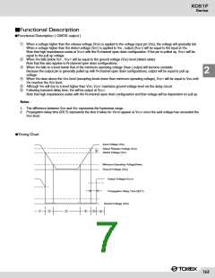
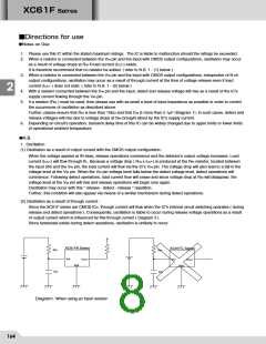
Further, please ensure that RIN is less than 10kΩ and that CIN is more than 0.1µF (Diagram 1). In such cases, detect and
release voltages will rise due to voltage drops at RIN brought about by the IC's supply current.�
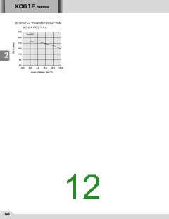
6. Depending on circuit's operation, transient delay time of this IC can be widely changed due to upper limits or lower limits
of operational ambient temparature.
ꢀN.B.
■備考�
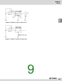
1. Oscillation
(1) Oscillation as a result of output current with the CMOS output configuration :
When the voltage applied at IN rises, release operations commence and the detector's output voltage increases. Load
current (IOUT) will flow through RL. Because a voltage drop ( RIN x IOUT) is produced at the RIN resistor, located between
the input (IN) and the VIN pin, the load current will flow via the IC's VIN pin. The voltage drop will also lead to a fall in the
voltage level at the VIN pin. When the VIN pin voltage level falls below the detect voltage level, detect operations will
commence. Following detect operations, load current flow will cease and since voltage drop at RIN will disappear, the
voltage level at the VIN pin will rise and release operations will begin over again.
Oscillation may occur with this " release - detect - release " repetition.
Further, this condition will also appear via means of a similar mechanism during detect operations.
(2) Oscillation as a result of through current :
Since the XC61F series are CMOS ICS, through current will flow when the IC's internal circuit switching operates ( during
release and detect operations ). Consequently, oscillation is liable to occur during release voltage operations as a result
of output current which is influenced by this through current ( Diagram 3 ).
Since hysteresis exists during detect operations, oscillation is unlikely to occur.
XC61FN Series
XC61FC Series
RIN
RIN
VIN
VOUT
VIN
VOUT
VSS
VSS
CIN
CIN
Diagram1. When using an input resistor
164

 TOREX [ Torex Semiconductor ]