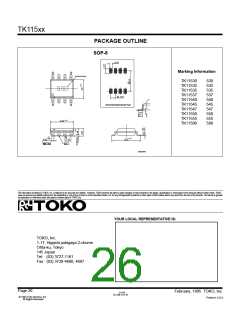
TK115xx
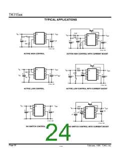
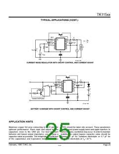
TYPICAL APPLICATIONS (CONT.)
39 Ω
1µF
R
S
S
S
S
S
S
1
2
3
4
8
7
6
5
V
O
R =
+
+
I
O
4.7
F
µ
S
Z
100K
+
_
V
IN
V
3
S
S
S
+
_
V
SW
S
S
GND
KT115xx • TA07
CURRENT MODE REGULATOR WITH ON/OFF CONTROL AND CURRENT BOOST
3.9 Ω
1µF
R
S
S
S
S
S
S
S
1
2
3
4
8
7
6
5
+
+
4.7µF
S
+
_
100K
S
+
_
S
S
S
S
S
Transistor On/Off control
KT115xx • TA08
BATTERY CHARGER WITH ON/OFF CONTROL AND CURRENT BOOST
APPLICATION HINTS
(ESR) should be taken into account. These parameters
can influence power supply noise and ripple rejection. In
extreme cases, oscillation may occur. In order to maintain
stability, the output bypass capacitor value should be
minimum 1 µF for Tantalum electrolytic or 4.7 µF for
Maximize copper foil area connecting to all IC pins for
optimum performance. Place input and output bypass
capacitors close to the GND pin. For best transient
behavior and lowest output impedance, use as large a
capacitor value as possible. The temperature coefficient
of the capacitance and Equivalent Series Resistance
o
Aluminum electrolytic at T = 25 C.
A
February, 1995 TOKO, Inc.
Page 25
10-15-94

 TOKO [ TOKO, INC ]