SN65HVD230
SN65HVD231
SN65HVD232
www.ti.com
SLOS346H–MARCH 2001–REVISED JULY 2006
APPLICATION INFORMATION (continued)
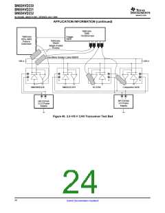
Driver
Input
CAN
Bus
Receiver
Output
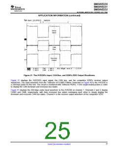
Figure 41. The HVD230's Input, CAN Bus, and X250's RXD Output Waveforms
Figure 41 displays the HVD230's input signal, the CAN bus, and the competitor X250's receiver output
waveforms. The input waveform from the Tektronix HFS-9003 Pattern Generator in Figure 40 to the HVD230 is
a 250-kbps pulse for this test. The circuit is monitored with Tektronix P6243, 1-GHz single-ended probes in order
to display the CAN dominant and recessive bus states.
Figure 41 displays the 250-kbps pulse input waveform to the HVD230 on channel 1. Channels 2 and 3 display
CANH and CANL respectively, with their recessive bus states overlaying each other to clearly display the
dominant and recessive CAN bus states. Channel 4 is the receiver output waveform of the competitor X250.
25
Submit Documentation Feedback

 TI [ TEXAS INSTRUMENTS ]