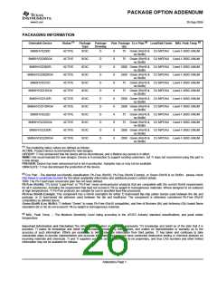
SN65HVD230
SN65HVD231
SN65HVD232
www.ti.com
SLOS346H–MARCH 2001–REVISED JULY 2006
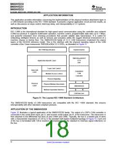
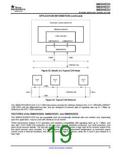
APPLICATION INFORMATION (continued)
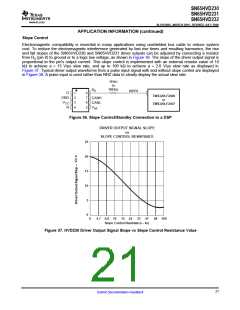
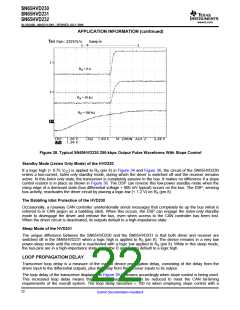
R
S
= 0 Ω
R
S
= 10 kΩ
R
S
= 100 kΩ
Figure 38. Typical SN65HVD230 250-kbps Output Pulse Waveforms With Slope Control
Standby Mode (Listen Only Mode) of the HVD230
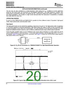
If a logic high (> 0.75 VCC) is applied to RS (pin 8) in Figure 34 and Figure 36, the circuit of the SN65HVD230
enters a low-current, listen only standby mode, during which the driver is switched off and the receiver remains
active. In this listen only state, the transceiver is completely passive to the bus. It makes no difference if a slope
control resistor is in place as shown in Figure 36. The DSP can reverse this low-power standby mode when the
rising edge of a dominant state (bus differential voltage > 900 mV typical) occurs on the bus. The DSP, sensing
bus activity, reactivates the driver circuit by placing a logic low (< 1.2 V) on RS (pin 8).
The Babbling Idiot Protection of the HVD230
Occasionally, a runaway CAN controller unintentionally sends messages that completely tie up the bus (what is
referred to in CAN jargon as a babbling idiot). When this occurs, the DSP can engage the listen-only standby
mode to disengage the driver and release the bus, even when access to the CAN controller has been lost.
When the driver circuit is deactivated, its outputs default to a high-impedance state.
Sleep Mode of the HVD231
The unique difference between the SN65HVD230 and the SN65HVD231 is that both driver and receiver are
switched off in the SN65HVD231 when a logic high is applied to RS (pin 8). The device remains in a very low
power-sleep mode until the circuit is reactivated with a logic low applied to RS (pin 8). While in this sleep mode,
the bus-pins are in a high-impedance state, while the D and R pins default to a logic high.
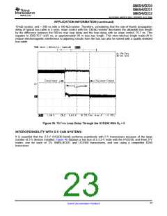
LOOP PROPAGATION DELAY
Transceiver loop delay is a measure of the overall device propagation delay, consisting of the delay from the
driver input to the differential outputs, plus the delay from the receiver inputs to its output.
The loop delay of the transceiver displayed in Figure 39 increases accordingly when slope control is being used.
This increased loop delay means that the total bus length must be reduced to meet the CAN bit-timing
requirements of the overall system. The loop delay becomes ≈ 100 ns when employing slope control with a
22
Submit Documentation Feedback

 TI [ TEXAS INSTRUMENTS ]