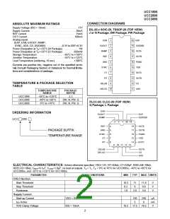
UCC1895
UCC2895
UCC3895
PIN DESCRIPTIONS
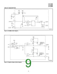
ADS: Adaptive Delay Set. This function sets the ratio be- DELAB, DELCD: Delay Programming Between
tween the maximum and minimum programmed output Complementary Outputs. DELAB programs the dead
delay dead time. When the ADS pin is directly connected time between switching of OUTA and OUTB, and DELCD
to the CS pin, no delay modulation occurs. The maximum programs the dead time between OUTC and OUTD. This
delay modulation occurs when ADS is grounded. In this delay is introduced between complementary outputs in
case, delay time is four times longer when CS = 0 than the same leg of the external bridge. The UCC3895 allows
when CS = 2.0V (the Peak Current threshold), ADS the user to select the delay, in which the resonant
changes the output voltage on the delay pins DELAB and switching of the external power stages takes place.
DELCD by the following formula:
Separate delays are provided for the two half-bridges to
accommodate differences in resonant capacitor charging
currents. The delay in each stage is set according to the
following formula:
(
)
VDEL =[0.75 • VCS − VADS ]+0.5V
where VCS and VADS are in Volts. ADS must be limited to
between 0V and 2.5V and must be less than or equal to
CS. DELAB and DELCD also will be clamped to a mini-
mum of 0.5V.
(25 • 10−12 )• RDEL
tDELAY
=
+ 25ns
VDEL
where VDEL is in Volts, and RDEL is in Ohms and tDELAY
is in seconds. DELAB and DELCD can source about
1mA maximum. Choose the delay resistors so that this
maximum is not exceeded. Programmable output delay
can be defeated by tying DELAB and/or DELCD to REF.
For an optimum performance keep stray capacitance on
these pins at <10pF.
EAOUT: Error Amplifier Output. It is also connected inter-
nally to the non-inverting input of the PWM comparator
and the no-load comparator. EAOUT is internally
clamped to the soft start voltage. The no-load comparator
shuts down the output stages when EAOUT falls below
500mV, and allows the outputs to turn-on again when
EAOUT rises above 600mV.
EAP: The non-inverting input to the error amplifier.
EAN: The inverting input to the error amplifier.
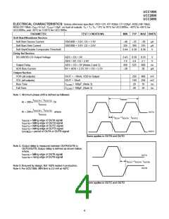
CT: Oscillator Timing Capacitor. (Refer to Fig. 1, Oscilla-
tor Block Diagram) The UCC3895’s oscillator charges CT
via a programmed current. The waveform on CT is a
sawtooth, with a peak voltage of 2.35V. The approximate
oscillator period is calculated by the following formula:
GND: Chip ground for all circuits except the output
stages.
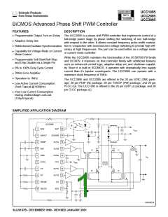
OUTA, OUTB, OUTC, OUTD: The 4 outputs are 100mA
complementary MOS drivers, and are optimized to drive
FET driver circuits. OUTA and OUTB are fully
complementary, (assuming no programmed delay). They
operate near 50% duty cycle and one-half the oscillating
frequency. OUTA and OUTB are intended to drive one
half-bridge circuit in an external power stage. OUTC and
OUTD will drive the other half-bridge and will have the
same characteristics as OUTA and OUTB. OUTC is
phase shifted with respect to OUTA, and OUTD is phase
shifted with respect to OUTB. Note that changing the
phase relationship of OUTC and OUTD with respect to
OUTA and OUTB requires other than the nominal 50%
duty ratio on OUTC and OUTD during those transients.
5 • RT • CT
tOSC
=
+120ns
48
where CT is in Farads, and RT is in Ohms and tOSC is in
seconds. CT can range from 100pF to 880pF. Please
note that a large CT and a small RT combination will re-
sult in extended fall times on the CT waveform. The in-
creased fall time will increase the SYNC pulse width,
hence limiting the maximum phase shift between OUTA,
OUTB and OUTC, OUTD outputs, which limits the maxi-
mum duty cycle of the converter.
CS: Current Sense. This is the inverting input of the Cur-
rent Sense comparator and the non-inverting input of the
Over-current comparator, and the ADS amplifier. The cur-
rent sense signal is used for cycle-by-cycle current limit-
ing in peak current mode control, and for overcurrent
protection in all cases with a secondary threshold for out-
put shutdown. An output disable initiated by an
overcurrent fault also results in a restart cycle, called
“soft stop”, with full soft start.
PGND: Output Stage Ground. To keep output switching
noise from critical analog circuits, the UCC3895 has 2
different ground connections. PGND is the ground
connection for the high-current output stages. Both GND
and PGND must be electrically tied together closely near
the IC. Also, since PGND carries high current, board
traces must be low impedance.
5

 TI [ TEXAS INSTRUMENTS ]