UC1907
UC2907
UC3907
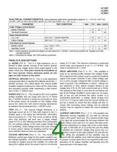
ELECTRICAL CHARACTERISTICS: Unless otherwise stated these specifications apply for TA = –55°C to +125°C for
UC1907; –40°C to +85°C for UC2907; and 0°C to +70°C for UC3907; VIN = 15V, TA=TJ.
PARAMETER
Under Voltage Lockout Section
Startup Threshold
TEST CONDITIONS
MIN
TYP
MAX UNITS
3.7
20
4.4
V
Threshold Hysteresis
Status Indicate Section
VOUT Low
mV
ADJ OUT = Current Share Bus
ADJ OUT = 1V, VOUT = 35V
0.2
0.1
0.5
5
V
Output Leakage
µA
Total Stand by Current Section
Startup Current
VIN = UVLO – 0.2V
VIN = 35V
3
6
5
mA
mA
Operating Current
10
Note 1: Unless otherwise specified all voltages are with respect to (–) SENSE. Currents are positive into, negative out of the
specified terminal.
Note 2: Guaranteed by design. Not 100% tested in production.
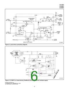
PIN/BLOCK DESCRIPTIONS
clamp of 2.0 Volts. The reference trimming is performed
closed loop, and measured at pin 11, (+) SENSE. The
value is trimmed to 2V ±1.25%.
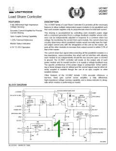
(–) SENSE (Pin 4) - This is a high-impedance pin in-
tended to allow remote sensing of the system ground,
bypassing any voltage drops which might appear in the
power return line. This point should be considered as
the “true” ground. Unless otherwise stated, all volt-
ages are with respect to this point.
DRIVE AMPLIFIER (Pins 8, 9, 12) - This amplifier is
used as an inverting buffer between the Voltage Ampli-
fier’s output and the medium used to couple the feedback
signal to the power controller. It has a fixed voltage gain
of 2.5 and is usually configured with a current-setting re-
sistor to ground. This establishes a current - sinking out-
put optimized to drive optical couplers biased at any
voltage from 4.5V to 35V, with current levels up to 20mA.
The polarity of this stage is such that an increasing volt-
age at the Voltage Amplifier’s sense input (as, for exam-
ple, at turn on) will increase the opto’s current. In a
nonisolated application, a voltage signal ranging from
0.25V to 4.1V may be taken from the current-setting out-
put but it should be noted that this voltage will also in-
crease with increasing sense voltage and an external
inverter may be required to obtain the correct feedback
polarity.
ARTIFICIAL GROUND (Pin 6) - This is a low impedance
circuit ground which is exactly 250 millivolts above the (–)
SENSE terminal. This offset allows the Ground Buffer
Amplifier negative headroom to return all the control bias
and operating currents while maintaining a high imped-
ance at the (–) SENSE input.
POWER RTN (Pin 5) - This should be the most negative
voltage available and can range from zero to 5V below
the (–) SENSE terminal. It should be connected as close
to the power source as possible so that voltage drops
across the return line and current sensing impedances
lie between this terminal and the (–) SENSE point.
VREF (Pin 7) - The internal Voltage Reference is a
band-gap circuit set at 2.0 Volts with respect to the (–)
SENSE input (1.75V above the ARTIFICIAL GROUND),
and an accuracy of ± 1.5%. This circuit, as well as all the
other chip functions, will work over a supply voltage
range of 4.5V to 35V allowing operation from unregulated
DC, an auxiliary voltage, or the same output voltage that
it is controlling. Under voltage lockout has been included
to insure proper startup by disabling internal bias cur-
rents until the reference rises into regulation.
CURRENT AMPLIFIER (Pins 1, 2, 3) - This amplifier has
differential sensing capability for use with an external
shunt in the power return line. The common-mode range
of its input will accommodate the full range between the
Power Return point and VCC–2V which will allow unde-
fined line impedances on either side of the current shunt.
The gain is internally set at 20 giving the user the ability
to establish the maximum voltage drop across the cur-
rent sense resistor at any value between 50 and 500 mil-
livolts. While the bandwidth of this amplifier may be
reduced with the addition of an external output capacitor
to ground, in most cases this is not required as the com-
pensation of the Adjust Amplifier will typically form the
dominant pole in the adjust loop.
VOLTAGE AMPLIFIER (Pins 11, 12) - This circuit is the
feedback control gain stage for the power module’s out-
put voltage regulation, and overall loop compensation will
normally be applied around this amplifier. Its output will
swing from slightly above the ground return to an internal
4

 TI [ TEXAS INSTRUMENTS ]