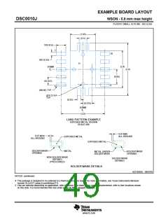
EXAMPLE BOARD LAYOUT
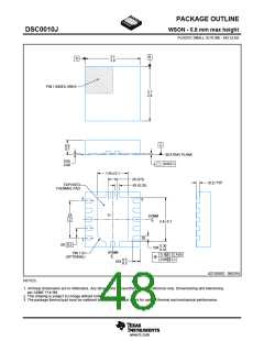
DSC0010J
WSON - 0.8 mm max height
PLASTIC SMALL OUTLINE - NO LEAD
(1.65)
(0.5)
10X (0.6)
1
10
10X (0.24)
11
(2.4)
(3.4)
SYMM
(0.95)
8X (0.5)
6
5
(R0.05) TYP
(
0.2) VIA
TYP
(0.25)
(0.575)
SYMM
(2.8)
LAND PATTERN EXAMPLE
EXPOSED METAL SHOWN
SCALE:20X
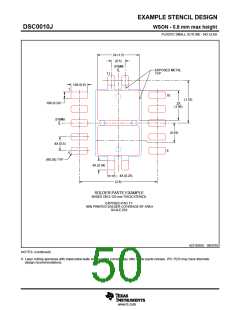
0.07 MIN
ALL AROUND
0.07 MAX
ALL AROUND
EXPOSED METAL
EXPOSED METAL
SOLDER MASK
OPENING
METAL
SOLDER MASK
OPENING
METAL UNDER
SOLDER MASK
NON SOLDER MASK
SOLDER MASK
DEFINED
DEFINED
(PREFERRED)
SOLDER MASK DETAILS
4221826/D 08/2018
NOTES: (continued)
4. This package is designed to be soldered to a thermal pad on the board. For more information, see Texas Instruments literature
number SLUA271 (www.ti.com/lit/slua271).
5. Vias are optional depending on application, refer to device data sheet. If any vias are implemented, refer to their locations shown
on this view. It is recommended that vias under paste be filled, plugged or tented.
www.ti.com

 TI [ TEXAS INSTRUMENTS ]