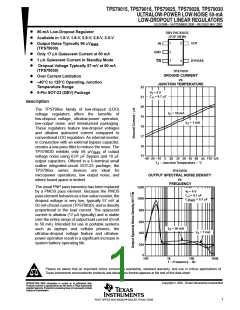
TPS79015, TPS79018, TPS79025, TPS79028, TPS79030
ULTRALOW-POWER LOW-NOISE 50-mA
LOW-DROPOUT LINEAR REGULATORS
SLVS299B – SEPTEMBER 2000 – REVISED MAY 2001
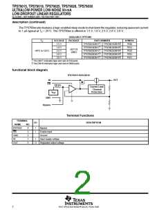
detail description
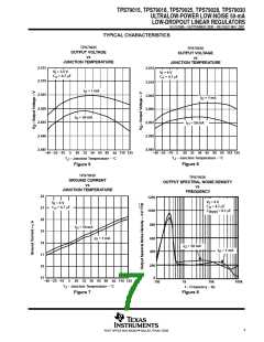
The TPS790xx uses a PMOS pass element to dramatically reduce both dropout voltage and supply current over
more conventional PNP-pass-element LDO designs. The PMOS pass element is a voltage-controlled device
and, unlike a PNP transistor, it does not require increased drive current as output current increases. Supply
current in the TPS790xx is essentially constant from no load to maximum load.
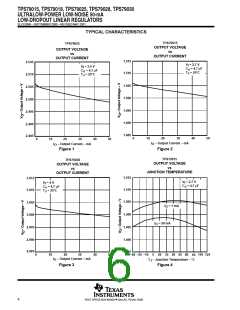
The TPS790xx family of low-dropout (LDO) regulators have been optimized for use in battery-operated
equipment. They feature extremely low dropout voltages, low output noise, low quiescent current (17 µA
typically), and enable inputs to reduce supply currents to 1 µA when the regulators are turned off.
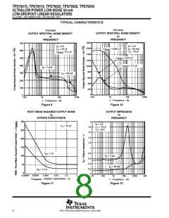
The internal voltage reference is a key source of noise in a LDO regulator. The TPS790xx has a BYPASS pin
which is connected to the voltage reference through a 150-kΩ internal resistor. The 150-kΩ internal resistor,
in conjunction with an external bypass capacitor connected to the BYPASS pin, creates a low pass filter to
reduce the voltage reference noise and, therefore, the noise at the regulator output. Note that the output will
startupslowerasthebypasscapacitanceincreasesduetotheRCtimeconstantatthebypasspinthatiscreated
by the internal 150-kΩ resistor and external capacitor.
Current limiting and thermal protection prevent damage by excessive output current and/or power dissipation.
The device switches into a constant-current mode at approximately 350 mA; further load reduces the output
voltage instead of increasing the output current. The thermal protection shuts the regulator off if the junction
temperature rises above approximately 165°C. Recovery is automatic when the junction temperature drops
approximately 25°C below the high temperature trip point. The PMOS pass element includes a back gate diode
that conducts reverse current when the input voltage level drops below the output voltage level.
A voltage of 1.7 V or greater on the EN input will disable the TPS790xx internal circuitry, reducing the supply
current to 1 µA. A voltage of less than 0.9 V on the EN input will enable the TPS790xx and will enable normal
operation to resume. The EN input does not include any deliberate hysteresis, and it exhibits an actual switching
threshold of approximately 1.5 V.
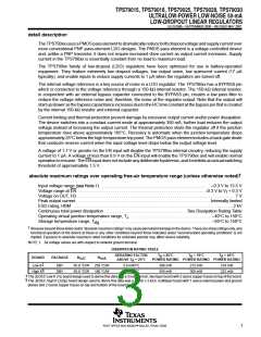
absolute maximum ratings over operating free-air temperature range (unless otherwise noted)
Input voltage range
. . . . . . . . . . . . . . . . . . . . . . . . . . . . . . . . . . . . . . . . . . . . . . . . . . –0.3 V to 13.5 V
Voltage range at EN . . . . . . . . . . . . . . . . . . . . . . . . . . . . . . . . . . . . . . . . . . . . . . . . . . . . . . . . . . . –0.3 V to V + 0.3 V
I
Voltage on OUT, FB . . . . . . . . . . . . . . . . . . . . . . . . . . . . . . . . . . . . . . . . . . . . . . . . . . . . . . . . . . . . . . . . . . . . . . . . . . 7 V
Peak output current . . . . . . . . . . . . . . . . . . . . . . . . . . . . . . . . . . . . . . . . . . . . . . . . . . . . . . . . . . . . . . Internally limited
ESD rating, HBM . . . . . . . . . . . . . . . . . . . . . . . . . . . . . . . . . . . . . . . . . . . . . . . . . . . . . . . . . . . . . . . . . . . . . . . . . . 2 kV
Continuous total power dissipation . . . . . . . . . . . . . . . . . . . . . . . . . . . . . . . . . . . . . See Dissipation Rating Table
Operating virtual junction temperature range, T . . . . . . . . . . . . . . . . . . . . . . . . . . . . . . . . . . . . . –40°C to 150°C
J
Storage temperature range, T
. . . . . . . . . . . . . . . . . . . . . . . . . . . . . . . . . . . . . . . . . . . . . . . . . . . –65°C to 150°C
stg
†
Stresses beyond those listed under “absolute maximum ratings” may cause permanent damage to the device. These are stress ratings only, and
functional operation of the device at these or any other conditions beyond those indicated under “recommended operating conditions” is not
implied. Exposure to absolute-maximum-rated conditions for extended periods may affect device reliability.
NOTE 1: All voltage values are with respect to network ground terminal.
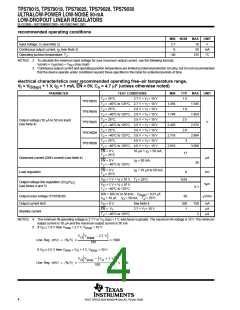
DISSIPATION RATING TABLE
DERATING FACTOR
T
A
≤ 25°C
T
A
= 70°C
T = 85°C
A
BOARD
PACKAGE
R
R
θJA
θJC
ABOVE T = 25°C
POWER RATING POWER RATING POWER RATING
A
‡
Low K
DBV
DBV
65.8 °C/W
65.8 °C/W
259 °C/W
180 °C/W
3.9 mW/°C
5.6 mW/°C
386 mW
555 mW
212 mW
305 mW
154 mW
222 mW
§
High K
‡
§
The JEDEC Low K (1s) board design used to derive this data was a 3 inch x 3 inch, two layer board with 2 ounce copper traces on top of the board.
The JEDEC High K (2s2p) board design used to derive this data was a 3 inch x 3 inch, multilayer board with 1 ounce internal power and ground
planes and 2 ounce copper traces on top and bottom of the board.
3
POST OFFICE BOX 655303 • DALLAS, TEXAS 75265

 TI [ TEXAS INSTRUMENTS ]