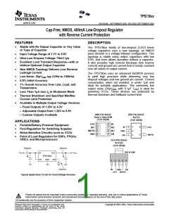
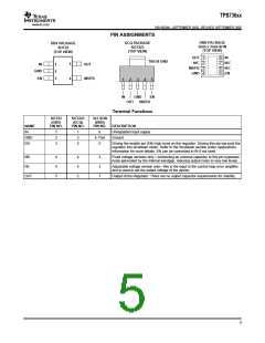
TPS736xx
www.ti.com
SBVS038K–SEPTEMBER 2003–REVISED SEPTEMBER 2005
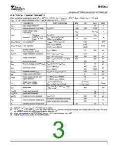
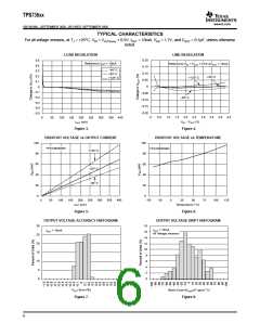
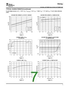
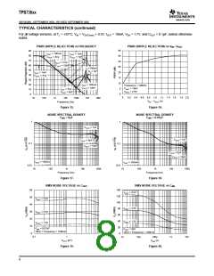
ELECTRICAL CHARACTERISTICS
Over operating temperature range (TJ = -40°C to +125°C), VIN = VOUT(nom) + 0.5V(1), IOUT = 10mA, VEN = 1.7V, and
COUT = 0.1µF, unless otherwise noted. Typical values are at TJ = 25°C.
PARAMETER
Input voltage range(1)(2)
TEST CONDITIONS
MIN
1.7
TYP
MAX
5.5
UNIT
V
VIN
VFB
Internal reference (TPS73601)
TJ = 25°C
1.198
1.20
1.210
V
Output voltage range
(TPS73601)
VFB
-0.5
-1.0
5.5 - VDO
+0.5
V
VOUT
Nominal
TJ = 25°C
Accuracy(1)
%
over VIN, IOUT
and T
,
VOUT + 0.5V ≤ VIN≤ 5.5V;
10mA ≤ IOUT≤ 400mA
±0.5
+1.0
∆VOUT%/∆VIN
Line regulation(1)
VO(nom) + 0.5V≤ VIN≤ 5.5V
1mA ≤ IOUT≤ 400mA
0.01
0.002
0.0005
%/V
∆VOUT%/∆IOUT Load regulation
%/mA
10mA ≤ IOUT≤ 400mA
Dropout voltage(3)
(VIN = VOUT(nom) - 0.1V)
VDO
IOUT = 400mA
75
200
mV
ZO(DO)
Output impedance in dropout
1.7V ≤ VIN≤ VOUT + VDO
VOUT = 0.9 × VOUT(nom)
3.6V ≤ VIN≤ 4.2V, 0°C ≤ TJ≤ 70°C
VOUT = 0V
0.25
650
Ω
400
500
800
800
mA
mA
mA
µA
ICL
Output current limit
ISC
Short-circuit current
Reverse leakage current(4) (-IIN
450
0.1
IREV
)
VEN ≤ 0.5V, 0V≤ VIN≤ VOUT
10
550
1000
1
IOUT = 10mA (IQ)
IOUT = 400mA
400
IGND
Ground pin current
µA
800
ISHDN
IFB
Shutdown current (IGND
)
VEN ≤ 0.5V, VOUT≤ VIN≤ 5.5
0.02
µA
µA
FB pin current (TPS73601)
0.1
0.3
f = 100Hz, IOUT = 400mA
f = 10KHz, IOUT = 400mA
COUT = 10µF, No CNR
58
Power-supply rejection ratio
(ripple rejection)
PSRR
dB
37
27 × VOUT
8.5 × VOUT
Output noise voltage
BW = 10Hz - 100KHz
VN
µVRMS
µs
COUT = 10µF, CNR = 0.01µF
VOUT = 3V, RL = 30Ω COUT = 1µF,
CNR = 0.01µF
tSTR
Startup time
600
VEN(HI)
VEN(LO)
IEN(HI)
Enable high (enabled)
1.7
0
VIN
0.5
0.1
V
V
Enable low (shutdown)
Enable pin current (enabled)
VEN = 5.5V
0.02
160
140
µA
Shutdown, temperature increasing
Reset, temperature decreasing
TSD
TJ
Thermal shutdown temperature
Operating junction temperature
°C
°C
-40
125
(1) Minimum VIN = VOUT +VDO or 1.7V, whichever is greater.
(2) For VOUT(nom) <1.6V, when VIN≤ 1.6V, the output will lock to VIN and may result in a damaging over-voltage level on the output. To avoid
this situation, disable the device before powering down the VIN
.
(3) VDO is not measured for the TPS73615 (VOUT(nom) = 1.5V) since minimum VIN = 1.7V.
(4) Refer to Applications section for more information.
3

 TI [ TEXAS INSTRUMENTS ]