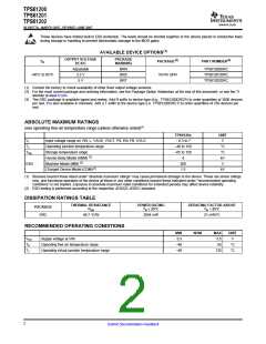
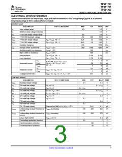
TPS61200
TPS61201
TPS61202
www.ti.com
SLVS577A–MARCH 2007–REVISED JUNE 2007
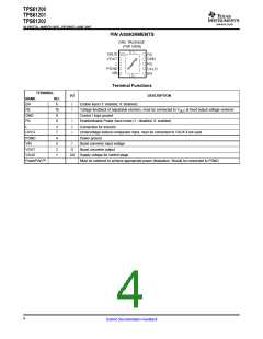
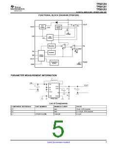
PIN ASSIGNMENTS
DRC PACKAGE
(TOP VIEW)
VAUX
FB
GND
VOUT
L
PS
PGND
VIN
UVLO
EN
Terminal Functions
TERMINAL
I/O
DESCRIPTION
NAME
EN
NO.
6
I
I
Enable input (1: enabled, 0: disabled).
FB
10
9
Voltage feedback of adjustable versions, must be connected to VOUT at fixed output voltage versions
Control / logic ground
GND
PS
8
I
I
I
Enable/disable Power Save mode (1 : disabled, 0: enabled)
Connection for Inductor
L
3
UVLO
PGND
VIN
7
Undervoltage lockout comparator input, must be connected to VAUX if not used
Power ground
4
5
I
Boost converter input voltage
VOUT
VAUX
PowerPAD™
2
O
Boost converter output
1
O/I
Supply voltage for control stage
Must be soldered to achieve appropriate power dissipation. Should be connected to PGND.
4
Submit Documentation Feedback

 TI [ TEXAS INSTRUMENTS ]