TPS562212
ZHCSNA3 –OCTOBER 2021
www.ti.com.cn
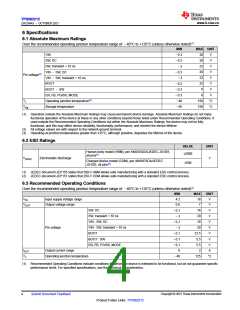
6.4 Thermal Information
TPS562212
THERMAL METRIC(1)
DRL (SOT-5X3)
UNIT
8 PINS
116.7
41.7
20.9
1.0
(2)
RθJA
RθJC(top)
RθJB
Junction-to-ambient thermal resistance
°C/W
°C/W
°C/W
°C/W
°C/W
°C/W
Junction-to-case (top) thermal resistance
Junction-to-board thermal resistance
Junction-to-top characterization parameter
Junction-to-board characterization parameter
Junction-to-ambient thermal resistance on TPS562212EVM
ΨJT
20.8
70
ΨJB
(3)
RθJC(EVM)
(1) For more information about traditional and new thermal metrics, see the Semiconductor and IC Package Thermal Metrics application
report, SPRA953
(2) The value of RθJA given in this table is only valid for comparison with other packages and can not be used for design purposes. These
values were simulated on a standard JEDEC board. They do not represent the performance obtained in an actual application.
(3) The real RθJA on the TPS562212EVM is about 70℃/W, test condition: VIN = 12 V, VOUT = 5 V, IOUT = 2 A, TA = 25℃.
6.5 Electrical Characteristics
Limits apply over the recommended operating junction temperature (TJ) range of –40°C to +125°C, unless otherwise stated.
Minimum and maximum limits are specified through test, design, or statistical correlation. Typical values represent the most
likely parametric norm at TJ = 25°C, and are provided for reference purposes only. Unless otherwise stated, the following
conditions apply: VIN = 4.2 V to 18 V.
PARAMETER
TEST CONDITIONS
MIN
TYP
MAX UNIT
SUPPLY
VIN
Operation input voltage
4.2
18
V
VIN quiescent current at power save
mode
Nonswitching, VEN = 1.2 V, VFB = 0.65 V,
IOUT = 0 mA
120
µA
IQ(VIN)
Nonswitching, VEN = 1.2 V, VFB = 0.65 V,
IOUT = 0 mA
VIN quiescent current at FCCM
VIN shutdown supply current
450
3
µA
µA
ISD(VIN)
UVLO
VIN = 12 V, VEN = 0 V
10
VUVLO(R)
VUVLO(F)
ENABLE
VEN(R)
VIN UVLO rising threshold
VIN UVLO falling threshold
VIN rising
VIN falling
3.8
3.4
4
4.2
3.8
V
V
3.6
EN voltage rising threshold
EN voltage falling threshold
EN rising, enable switching
EN falling, disable switching
1.05
0.91
1.15
1.01
1.25
1.10
V
V
VEN(F)
EN pin sourcing current pre EN rising
threshold
IEN(P1)
IEN(H)
VEN = 1.0 V
0.93
2.4
1.2
3.1
1.5
µA
µA
EN pin sourcing current hysteresis
3.81
REFERENCE VOLTAGE
TJ = 25°C
0.594
0.591
–0.1
0.6
0.6
0
0.606
0.609
0.1
V
V
VFB
FB voltage
TJ = –40°C to 125°C, VIN = 12 V
VFB = 0.65 V, TJ = 25°C
IFB(LKG)
STARTUP
ISS
FB input leakage current
µA
Soft-start charge current
VSS = 0 V
4.5
1.5
6.6
2
8.3
2.6
µA
ms
From first switching pulse until target
VOUT
tSS
Internal fixed soft-start time
SWITCHING FREQUENCY
fSW(FCCM)
Switching frequency, FCCM operation
1100
1200
66
1300
kHz
POWER STAGE
RDSON(HS)
High-side MOSFET on-resistance
TJ = 25°C, VIN = 12 V, VBOOT-SW = 5 V
mΩ
Copyright © 2021 Texas Instruments Incorporated
Submit Document Feedback
5
Product Folder Links: TPS562212

 TI [ TEXAS INSTRUMENTS ]