TPS562212
ZHCSNA3 –OCTOBER 2021
www.ti.com.cn
9 Power Supply Recommendations
The devices are designed to operate from an input voltage supply range between 4.2 V and 18 V. This input
supply must be well regulated. If the input supply is located more than a few inches from the device or converter,
additional bulk capacitance can be required in addition to the ceramic bypass capacitors. An electrolytic
capacitor with a value of 47 μF is a typical choice.
10 Layout
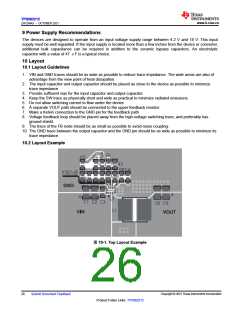
10.1 Layout Guidelines
1. VIN and GND traces should be as wide as possible to reduce trace impedance. The wide areas are also of
advantage from the view point of heat dissipation.
2. The input capacitor and output capacitor should be placed as close to the device as possible to minimize
trace impedance.
3. Provide sufficient vias for the input capacitor and output capacitor.
4. Keep the SW trace as physically short and wide as practical to minimize radiated emissions.
5. Do not allow switching current to flow under the device.
6. A separate VOUT path should be connected to the upper feedback resistor.
7. Make a Kelvin connection to the GND pin for the feedback path.
8. Voltage feedback loop should be placed away from the high-voltage switching trace, and preferably has
ground shield.
9. The trace of the FB node should be as small as possible to avoid noise coupling.
10. The GND trace between the output capacitor and the GND pin should be as wide as possible to minimize its
trace impedance.
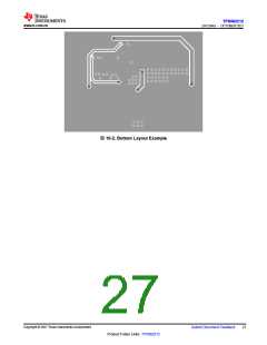
10.2 Layout Example
图10-1. Top Layout Example
Copyright © 2021 Texas Instruments Incorporated
26
Submit Document Feedback
Product Folder Links: TPS562212

 TI [ TEXAS INSTRUMENTS ]