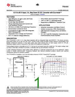
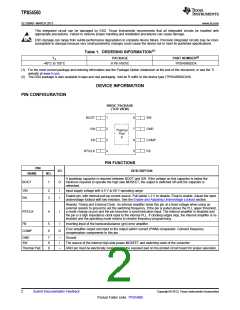
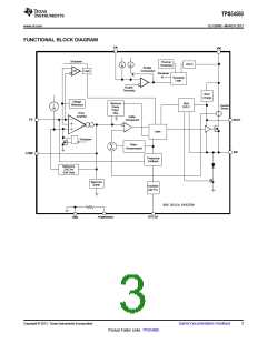
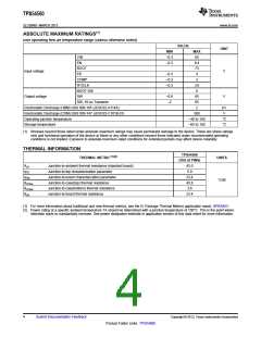
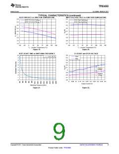
TPS54560
www.ti.com
SLVSBN0 –MARCH 2013
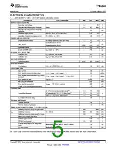
ELECTRICAL CHARACTERISTICS
TJ = –40°C to 150°C, VIN = 4.5 to 60V (unless otherwise noted)
PARAMETER
TEST CONDITIONS
MIN
TYP
MAX
UNIT
SUPPLY VOLTAGE (VIN PIN)
Operating input voltage
4.5
4.1
60
V
V
Internal undervoltage lockout threshold
Rising
4.3
4.48
Internal undervoltage lockout threshold
hysteresis
325
mV
Shutdown supply current
EN = 0 V, 25°C, 4.5 V ≤ VIN ≤ 60 V
2.25
146
4.5
μA
Operating: nonswitching supply current
FB = 0.83 V, TA = 25°C
175
ENABLE AND UVLO (EN PIN)
Enable threshold voltage
No voltage hysteresis, rising and falling
Enable threshold +50 mV
1.1
1.2
–4.6
–1.2
–3.4
540
1.3
V
Input current
μA
Enable threshold –50 mV
–0.58
–2.2
-1.8
-4.5
Hysteresis current
Enable to COMP active
INTERNAL SOFT-START TIME
Soft-Start Time
μA
VIN = 12 V, TA = 25°C
µs
fSW = 500 kHz, 10% to 90%
fSW = 2.5 MHz, 10% to 90%
2.1
ms
ms
Soft-Start Time
0.42
VOLTAGE REFERENCE
Voltage reference
0.792
0.8
92
0.808
190
V
HIGH-SIDE MOSFET
On-resistance
VIN = 12 V, BOOT-SW = 6 V
mΩ
ERROR AMPLIFIER
Input current
50
nA
Error amplifier transconductance (gM)
–2 μA < ICOMP < 2 μA, VCOMP = 1 V
–2 μA < ICOMP < 2 μA, VCOMP = 1 V, VFB = 0.4 V
VFB = 0.8 V
350
μMhos
Error amplifier transconductance (gM) during
soft-start
77
μMhos
Error amplifier dc gain
10,000
2500
±30
V/V
kHz
μA
Min unity gain bandwidth
Error amplifier source/sink
COMP to SW current transconductance
V(COMP) = 1 V, 100 mV overdrive
17
A/V
CURRENT LIMIT
All VIN and temperatures, Open Loop(1)
All temperatures, VIN = 12 V, Open Loop(1)
VIN = 12 V, TA = 25°C, Open Loop(1)
6.3
6.3
7.1
7.5
7.5
7.5
60
8.8
8.3
7.9
Current limit threshold
A
Current limit threshold delay
ns
THERMAL SHUTDOWN
Thermal shutdown
176
12
°C
°C
Thermal shutdown hysteresis
TIMING RESISTOR AND EXTERNAL CLOCK (RT/CLK PIN)
Switching frequency range using RT mode
100
450
160
2500
550
kHz
kHz
kHz
ns
fSW
Switching frequency
RT = 200 kΩ
500
Switching frequency range using CLK mode
Minimum CLK input pulse width
RT/CLK high threshold
2300
15
1.55
1.2
1.7
V
RT/CLK low threshold
0.5
V
RT/CLK falling edge to SW rising edge
delay
Measured at 500 kHz with RT resistor in series
Measured at 500 kHz
55
78
ns
PLL lock in time
μs
(1) Open Loop current limit measured directly at the SW pin and is independent of the inductor value and slope compensation.
Copyright © 2013, Texas Instruments Incorporated
Submit Documentation Feedback
5
Product Folder Links: TPS54560

 TI [ TEXAS INSTRUMENTS ]