TPS54332
SLVS875B –JANUARY 2009–REVISED FEBRUARY 2012
www.ti.com
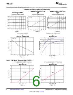
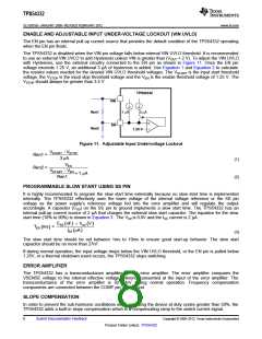
ENABLE AND ADJUSTABLE INPUT UNDER-VOLTAGE LOCKOUT (VIN UVLO)
The EN pin has an internal pull-up current source that provides the default condition of the TPS54332 operating
when the EN pin floats.
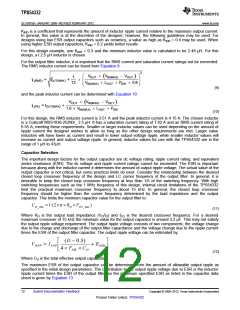
The TPS54332 is disabled when the VIN pin voltage falls below internal VIN UVLO threshold. It is recommended
to use an external VIN UVLO to add Hysteresis unless VIN is greater than (VOUT + 2 V). To adjust the VIN UVLO
with Hysteresis, use the external circuitry connected to the EN pin as shown in Figure 11. Once the EN pin
voltage exceeds 1.25 V, an additional 3 μA of hysteresis is added. Use Equation 1 and Equation 2 to calculate
the resistor values needed for the desired VIN UVLO threshold voltages. The VSTART is the input start threshold
voltage, the VSTOP is the input stop threshold voltage and the VEN is the enable threshold voltage of 1.25 V. The
VSTOP should always be greater than 3.5 V.
TPS54332
VIN
Ren1
Ren2
1 mA
3 mA
+
-
EN
1.25 V
Figure 11. Adjustable Input Undervoltage Lockout
VSTART - VSTOP
Ren1 =
3 mA
(1)
(2)
VEN
Ren2 =
VSTART - V
EN + 1 mA
Ren1
PROGRAMMABLE SLOW START USING SS PIN
It is highly recommended to program the slow start time externally because no slow start time is implemented
internally. The TPS54332 effectively uses the lower voltage of the internal voltage reference or the SS pin
voltage as the power supply’s reference voltage fed into the error amplifier and will regulate the output
accordingly. A capacitor (CSS) on the SS pin to ground implements a slow start time. The TPS54332 has an
internal pull-up current source of 2 μA that charges the external slow start capacitor. The equation for the slow
start time (10% to 90%) is shown in Equation 3 . The Vref is 0.8V and the ISS current is 2 μA.
CSS nF ´ V
V
( ) ref ( )
TSS ms =
( )
ISS mA
( )
(3)
The slow start time should be set between 1ms to 10ms to ensure good start-up behavior. The slow start
capacitor should be no more than 27nF.
If during normal operation, the input voltage drops below the VIN UVLO threshold, or the EN pin is pulled below
1.25V, or a thermal shutdown event occurs, the TPS54332 stops switching.
ERROR AMPLIFIER
The TPS54332 has a transconductance amplifier for the error amplifier. The error amplifier compares the
VSENSE voltage to the internal effective voltage reference presented at the input of the error amplifier. The
transconductance of the error amplifier is 92 μA/V during normal operation. Frequency compensation
components are connected between the COMP pin and ground.
SLOPE COMPENSATION
In order to prevent the sub-harmonic oscillations when operating the device at duty cycles greater than 50%, the
TPS54332 adds a built-in slope compensation which is a compensating ramp to the switch current signal.
8
Submit Documentation Feedback
Copyright © 2009–2012, Texas Instruments Incorporated
Product Folder Link(s): TPS54332

 TI [ TEXAS INSTRUMENTS ]