TPS2148
TPS2158
SLVS373 – AUGUST 2001
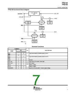
detailed description
VIN/SWIN1
The VIN/SWIN1 serves as the input to the internal LDO and as the input to one N-channel MOSFET. The 3.3-V
LDO has a dropout voltage of 0.35 V and is rated for 200 mA of continuous current. The power switch is an
N-channel MOSFET with a maximum on-state resistance of 580 mΩ. Configured as a high-side switch, the
power switch prevents current flow from OUT to IN and IN to OUT when disabled. The power switch is rated
at 150 mA, continuous current. VIN/SWIN1 must be connected to a voltage source for device operation.
OUTx
OUT1 and OUT2 are the outputs from the internal power-distribution switches.
LDO_OUT
LDO_OUT is the output of the internal 200-mA LDO. It is also the input to a second power switch. This power
switch in an N-channel MOSFET with a maximum on-state resistance of 580 mΩ. Configured as a high-side
switch, the power switch prevents current flow from OUT to IN and IN to OUT when disabled. The power switch
is rated at 150 mA, continuous current.
LDO_EN
The active high input, LDO_EN, is used to enable the internal LDO and is compatible with TTL and CMOS logic.
enable (ENx, ENx)
The logic enable disables the power switch. Both switches have independent enables and are compatible with
both TTL and CMOS logic.
current sense
A sense FET monitors the current supplied to the load. Current is measured more efficiently by the sense FET
than by conventional resistance methods. When an overload or short circuit is encountered, the current-sense
circuitry sends a control signal to the driver. The driver in turn reduces the gate voltage and drives the power
FET into its saturation region, which switches the output into a constant-current mode and holds the current
constant while varying the voltage on the load.
thermal sense
A dual-threshold thermal trip is implemented to allow fully independent operation of the power distribution
switches. In an overcurrent or short-circuit condition, the junction temperature rises. When the die temperature
rises to approximately 120°C, the internal thermal sense circuitry determines which power switch is in an
overcurrent condition and turns off that switch, thus isolating the fault without interrupting operation of the
adjacent power switch. Because hysteresis is built into the thermal sense, the switch turns back on after the
device has cooled approximately 10 degrees. The switch continues to cycle off and on until the fault is removed.
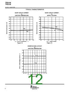
undervoltage lockout
Avoltagesensecircuitmonitorstheinputvoltage. Whentheinputvoltageisbelowapproximately2.5V, acontrol
signal turns off the power switch.
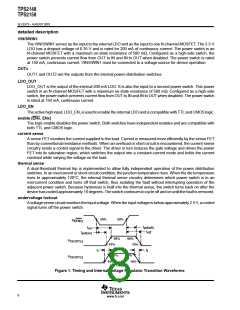
50%
50%
V
I(ENx)
t
t
pd(off)
on
pd(on)
t
t
off
90%
10%
90%
10%
V
V
O(OUTx)
t
t
f
r
90%
10%
90%
10%
O(OUTx)
TIMING
Figure 1. Timing and Internal Voltage Regulator Transition Waveforms
8
www.ti.com

 TI [ TEXAS INSTRUMENTS ]