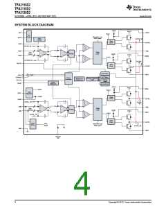
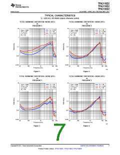
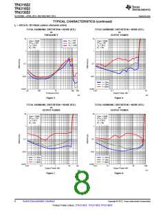
TPA3116D2
TPA3118D2
TPA3130D2
SLOS708B –APRIL 2012–REVISED MAY 2012
www.ti.com
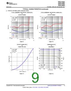
SYSTEM BLOCK DIAGRAM
GVDD
PVCC
BSPR
SDZ
PVCC
TTL
Buffer
Modulation and
PBTL Select
MUTE
Gain
Control
OUTPR_FB
Gate
Drive
OUTPR
GAIN
+
OUTPR FB
–
–
–
–
GND
RINP
+
+
PWM
Logic
Gain
Control
PLIMIT
GVDD
–
PVCC
–
RINN
+
BSNR
+
PVCC
OUTPNR FB
FAULTZ
OUTNR_
FB
+
Gate
Drive
OUTNR
GND
SC Detect
DC Detect
SYNC
GAIN/SLV
Ramp
Generator
Startup Protection
Logic
Biases and
References
Thermal
Detect
AM<2:0>
PLIMIT
Reference
PLIMIT
UVLO/OVLO
GVDD
PVCC
BSNL
AVDD
PVCC
LDO
Regulator
AVCC
GVDD
Gate
Drive
OUTNL
GVDD
+
OUTNL_FB
OUTNL_
FB
–
–
–
LINN
GND
+
Gain
Control
PWM
Logic
PLIMIT
GVDD
–
LINP
PVCC
+
+
+
BSPL
PVCC
OUTPL_FB
–
Gate
Drive
OUTPL
GND
Input
PBTL
Modulation and
PBTL Select
Sense
Select
OUTPL_FB
GND
Thermal
Pad
4
Copyright © 2012, Texas Instruments Incorporated

 TI [ TEXAS INSTRUMENTS ]