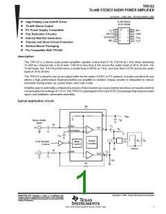
TPA152
75-mW STEREO AUDIO POWER AMPLIFIER
SLOS210A – JUNE 1998 – REVISED MARCH 2000
‡
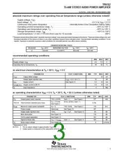
absolute maximum ratings over operating free-air temperature range (unless otherwise noted)
Supply voltage, V
. . . . . . . . . . . . . . . . . . . . . . . . . . . . . . . . . . . . . . . . . . . . . . . . . . . . . . . . . . . . . . . . . . . . . . . . 6 V
DD
Input voltage , V . . . . . . . . . . . . . . . . . . . . . . . . . . . . . . . . . . . . . . . . . . . . . . . . . . . . . . . . . . . –0.3 V to V + 0.3 V
I
DD
Continuous total power dissipation . . . . . . . . . . . . . . . . . . . . . internally limited (See Dissipation Rating Table)
Operating junction temperature range, T . . . . . . . . . . . . . . . . . . . . . . . . . . . . . . . . . . . . . . . . . . –40°C to 150° C
J
Operating case temperature range, T
. . . . . . . . . . . . . . . . . . . . . . . . . . . . . . . . . . . . . . . . . . . . –40°C to 125° C
C
Storage temperature range, T
. . . . . . . . . . . . . . . . . . . . . . . . . . . . . . . . . . . . . . . . . . . . . . . . . . –65°C to 150°C
Lead temperature 1,6 mm (1/16 inch) from case for 10 seconds . . . . . . . . . . . . . . . . . . . . . . . . . . . . . . . 260°C
stg
†
Stresses beyond those listed under “absolute maximum ratings” may cause permanent damage to the device. These are stress ratings only, and
functional operation of the device at these or any other conditions beyond those indicated under “recommended operating conditions” is not
implied. Exposure to absolute-maximum-rated conditions for extended periods may affect device reliability.
DISSIPATION RATING TABLE
PACKAGE
T
A
≤ 25°C
DERATING FACTOR
T
A
= 70°C
T = 85°C
A
D
724 mW
5.8 mW/°C
464 mW
376 mW
recommended operating conditions
MIN
4.5
MAX
5.5
UNIT
V
Supply voltage, V
DD
Operating free-air temperature, T
–40
85
°C
A
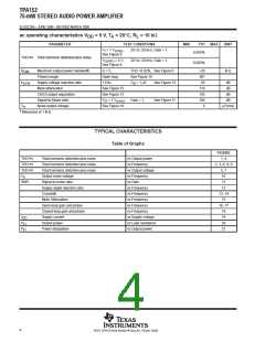
dc electrical characteristics at T = 25°C, V
= 5 V
DD
A
PARAMETER
TEST CONDITIONS
MIN
TYP
MAX
UNIT
mV
dB
V
OO
Output offset voltage
Supply ripple rejection ratio
Supply current
10
V
= 4.9 V to 5.1 V
DD
See Figure 13
81
5.5
5.5
>1
I
I
14
14
mA
mA
MΩ
DD
Supply current in MUTE
Input impedance
DD(MUTE)
Z
I
ac operating characteristics V
= 5 V, T = 25°C, R = 32 Ω (unless otherwise noted)
DD
A
L
PARAMETER
TEST CONDITIONS
MIN
TYP
MAX
UNIT
†
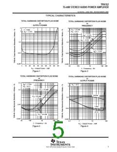
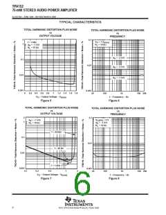
75
P
O
Output power (each channel)
THD ≤ 0.03%,
Gain = 1,
See Figure 1
mW
P
= 75 mW,
20 Hz–20 kHz, Gain = 1,
O
THD+N Total harmonic distortion plus noise
0.2%
See Figure 2
B
OM
Maximum output power bandwidth
Phase margin
A
= 5,
THD <0.6%, See Figure 2
See Figure 16
>20
80°
65
kHz
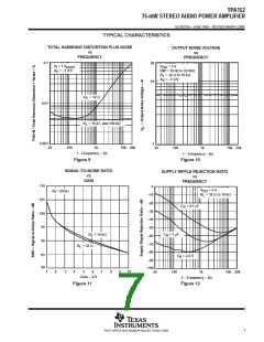
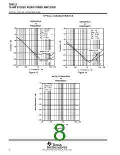
V
Open loop,
1 kHz,
Supply ripple rejection ratio
Mute attenuation
C
= 1 µF,
See Figure 12
dB
dB
B
See Figure 15
See Figure 13
110
102
104
6
Ch/Ch output separation
Signal-to-Noise ratio
dB
V
O
= 1 V
,
Gain = 1
See Figure 11
dB
(rms)
V
n
Noise output voltage
See Figure 10
µV(rms)
†
Measured at 1 kHz.
NOTES: 1. The dc output voltage is approximately V /2.
DD
2. Output power is measured at the output pins of the IC at 1 kHz.
3
POST OFFICE BOX 655303 • DALLAS, TEXAS 75265

 TI [ TEXAS INSTRUMENTS ]