TMS570LS3137
www.ti.com
SPNS162.–SEPTEMBER 2011
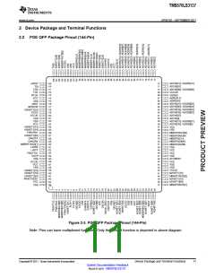
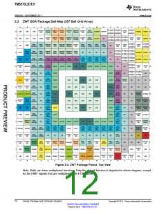
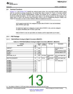
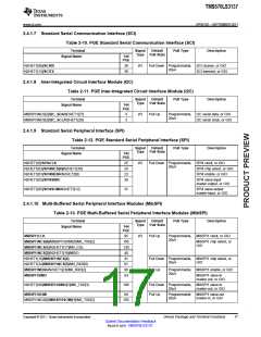
2.4 Terminal Functions
Section 2.4.1 and Section 2.4.2 identify the external signal names, the associated pin/ball numbers along
with the mechanical package designator, the pin/ball type (Input, Output, IO, Power or Ground), whether
the pin/ball has any internal pullup/pulldown, whether the pin/ball can be configured as a GIO, and a
functional pin/ball description. The first signal name listed is the primary function for that terminal. The
signal name in Bold is the function being described. Refer to the I/O Multiplexing Module (IOMM) User
Guide for information on how to select between different multiplexed functions.
NOTE
All I/O signals except nRST are configured as inputs while nPORRST is low and immediately
after nPORRST goes High.
All output-only signals are configured as inputs while nPORRST is low, and are configured
as outputs immediately after nPORRST goes High.
While nPORRST is low, the input buffers are disabled, and the output buffers are tri-stated.
2.4.1 PGE Package
2.4.1.1 Multi-Buffered Analog-to-Digital Converters (MibADC)
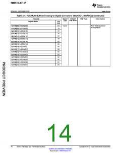
Table 2-4. PGE Multi-Buffered Analog-to-Digital Converters (MibADC1, MibADC2)
Terminal
Signal
Type
Default
Pull State
Pull Type
Description
Signal Name
144
PGE
ADREFHI(1)
66
Input
-
-
ADC high reference
supply
ADREFLO(1)
VCCAD(1)
VSSAD(1)
67
69
68
86
Input
Power
Ground
ADC low reference supply
Operating supply for ADC
AD1EVT/MII_RX_ER
Input Pull Down Programmable, ADC1 event trigger input,
20uA or GIO
MIBSPI3NCS[0]/AD2EVT
55
I/O
Pull Up
Programmable, ADC2 event trigger input,
20uA
or GIO
AD1IN[0]
60
71
73
74
76
78
80
61
Input
-
-
ADC1 analog input
AD1IN[01]
AD1IN[02]
AD1IN[03]
AD1IN[04]
AD1IN[05]
AD1IN[06]
AD1IN[07]
(1) The ADREFHI, ADREFLO, VCCAD and VSSAD connections are common for both ADC cores.
Device Package and Terminal Functions
Copyright © 2011, Texas Instruments Incorporated
13
Submit Documentation Feedback
focus.ti.com: TMS570LS3137

 TI [ TEXAS INSTRUMENTS ]