TMS320F28335, TMS320F28334, TMS320F28332
TMS320F28235, TMS320F28234, TMS320F28232
SPRS439M –JUNE 2007–REVISED AUGUST 2012
www.ti.com
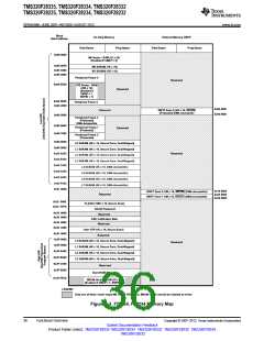
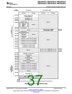
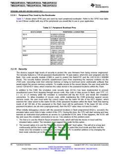
The wait-states for the various spaces in the memory map area are listed in Table 3-5.
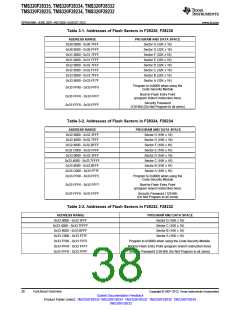
Table 3-5. Wait-states
WAIT-STATES
(CPU)
WAIT-STATES
(DMA)(1)
AREA
COMMENTS
M0 and M1 SARAMs
Peripheral Frame 0
0-wait
Fixed
0-wait (writes)
1-wait (reads)
0-wait (writes)
2-wait (reads)
0-wait (writes)
2-wait (reads)
0-wait (reads)
No access (writes)
0-wait (writes)
1-wait (reads)
No access
Peripheral Frame 3
Peripheral Frame 1
Assumes no conflicts between CPU and DMA.
Cycles can be extended by peripheral generated ready.
Consecutive (back-to-back) writes to Peripheral Frame 1
registers will experience a 1-cycle pipeline hit (1-cycle delay)
Peripheral Frame 2
0-wait (writes)
2-wait (reads)
0-wait
No access
No access
Fixed. Cycles cannot be extended by the peripheral.
L0 SARAM
L1 SARAM
L2 SARAM
L3 SARAM
L4 SARAM
L5 SARAM
L6 SARAM
Assumes no CPU conflicts
0-wait data (reads)
0-wait data (writes)
0-wait
Assumes no conflicts between CPU and DMA.
1-wait program
(reads)
L7 SARAM
XINTF
1-wait program
(writes)
Programmable
Programmable
Programmed via the XTIMING registers or extendable via
external XREADY signal to meet system timing requirements.
1-wait is minimum wait states allowed on external waveforms
for both reads and writes on XINTF.
0-wait minimum writes 0-wait minimum writes 0-wait minimum for writes assumes write buffer enabled and
with write buffer
enabled
with write buffer enabled not full.
Assumes no conflicts between CPU and DMA. When DMA and
CPU attempt simultaneous conflict, 1-cycle delay is added for
arbitration.
OTP
Programmable
1-wait minimum
No access
No access
Programmed via the Flash registers.
1-wait is minimum number of wait states allowed. 1-wait-state
operation is possible at a reduced CPU frequency.
FLASH
Programmable
Programmed via the Flash registers.
1-wait Paged min
0-wait minimum for paged access is not allowed
1-wait Random min
Random ≥ Paged
FLASH Password
Boot-ROM
16-wait fixed
1-wait
No access
No access
Wait states of password locations are fixed.
0-wait speed is not possible.
(1) The DMA has a base of 4 cycles/word.
40
Functional Overview
Copyright © 2007–2012, Texas Instruments Incorporated
Submit Documentation Feedback
Product Folder Link(s): TMS320F28335 TMS320F28334 TMS320F28332 TMS320F28235 TMS320F28234
TMS320F28232

 TI [ TEXAS INSTRUMENTS ]