TMS320F28335, TMS320F28334, TMS320F28332
TMS320F28235, TMS320F28234, TMS320F28232
www.ti.com
SPRS439M –JUNE 2007–REVISED AUGUST 2012
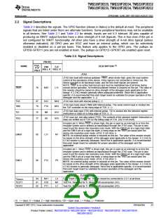
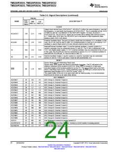
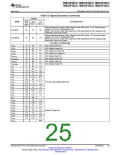
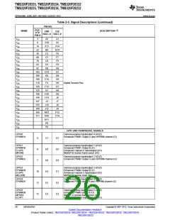
2.2 Signal Descriptions
Table 2-3 describes the signals. The GPIO function (shown in Italics) is the default at reset. The peripheral
signals that are listed under them are alternate functions. Some peripheral functions may not be available
in all devices. See Table 2-1 and Table 2-2 for details. Inputs are not 5-V tolerant. All pins capable of
producing an XINTF output function have a drive strength of 8 mA (typical). This is true even if the pin is
not configured for XINTF functionality. All other pins have a drive strength of 4-mA drive typical (unless
otherwise indicated). All GPIO pins are I/O/Z and have an internal pullup, which can be selectively
enabled or disabled on a per-pin basis. This feature only applies to the GPIO pins. The pullups on
GPIO0–GPIO11 pins are not enabled at reset. The pullups on GPIO12–GPIO87 are enabled upon reset.
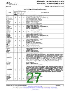
Table 2-3. Signal Descriptions
PIN NO.
(1)
PGF,
PTP
PIN #
NAME
DESCRIPTION
ZHH
ZJZ
BALL # BALL #
JTAG
JTAG test reset with internal pulldown. TRST, when driven high, gives the scan system
control of the operations of the device. If this signal is not connected or driven low, the
device operates in its functional mode, and the test reset signals are ignored.
NOTE: TRST is an active high test pin and must be maintained low at all times during
normal device operation. An external pulldown resistor is required on this pin. The value of
this resistor should be based on drive strength of the debugger pods applicable to the
design. A 2.2-kΩ resistor generally offers adequate protection. Since this is application-
specific, it is recommended that each target board be validated for proper operation of the
debugger and the application. (I, ↓)
TRST
78
M10
L11
TCK
TMS
87
79
N12
P10
M14
M12
JTAG test clock with internal pullup (I, ↑)
JTAG test-mode select (TMS) with internal pullup. This serial control input is clocked into
the TAP controller on the rising edge of TCK. (I, ↑)
JTAG test data input (TDI) with internal pullup. TDI is clocked into the selected register
(instruction or data) on a rising edge of TCK. (I, ↑)
TDI
76
77
M9
K9
N12
N13
JTAG scan out, test data output (TDO). The contents of the selected register (instruction or
data) are shifted out of TDO on the falling edge of TCK. (O/Z 8 mA drive)
TDO
Emulator pin 0. When TRST is driven high, this pin is used as an interrupt to or from the
emulator system and is defined as input/output through the JTAG scan. This pin is also
used to put the device into boundary-scan mode. With the EMU0 pin at a logic-high state
and the EMU1 pin at a logic-low state, a rising edge on the TRST pin would latch the
device into boundary-scan mode. (I/O/Z, 8 mA drive ↑)
NOTE: An external pullup resistor is required on this pin. The value of this resistor should
be based on the drive strength of the debugger pods applicable to the design. A 2.2-kΩ to
4.7-kΩ resistor is generally adequate. Since this is application-specific, it is recommended
that each target board be validated for proper operation of the debugger and the
application.
EMU0
85
L11
N7
Emulator pin 1. When TRST is driven high, this pin is used as an interrupt to or from the
emulator system and is defined as input/output through the JTAG scan. This pin is also
used to put the device into boundary-scan mode. With the EMU0 pin at a logic-high state
and the EMU1 pin at a logic-low state, a rising edge on the TRST pin would latch the
device into boundary-scan mode. (I/O/Z, 8 mA drive ↑)
NOTE: An external pullup resistor is required on this pin. The value of this resistor should
be based on the drive strength of the debugger pods applicable to the design. A 2.2-kΩ to
4.7-kΩ resistor is generally adequate. Since this is application-specific, it is recommended
that each target board be validated for proper operation of the debugger and the
application.
EMU1
86
P12
P8
FLASH
VDD3VFL
TEST1
TEST2
84
81
82
M11
K10
P11
L9
M7
L7
3.3-V Flash Core Power Pin. This pin should be connected to 3.3 V at all times.
Test Pin. Reserved for TI. Must be left unconnected. (I/O)
Test Pin. Reserved for TI. Must be left unconnected. (I/O)
(1) I = Input, O = Output, Z = High impedance, OD = Open drain, ↑ = Pullup, ↓ = Pulldown
Copyright © 2007–2012, Texas Instruments Incorporated
Introduction
23
Submit Documentation Feedback
Product Folder Link(s): TMS320F28335 TMS320F28334 TMS320F28332 TMS320F28235 TMS320F28234
TMS320F28232

 TI [ TEXAS INSTRUMENTS ]