PDF
最近搜索
热门搜索
发布采购

| 型号: | TMDS261 |
| PDF下载: | 下载PDF文件 查看货源 |
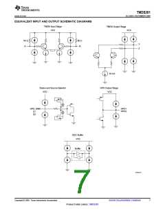
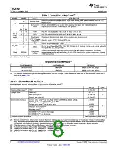
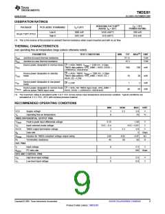
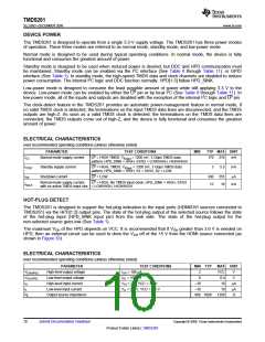
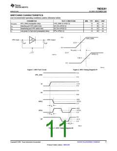
| 内容描述: | 1080 - 色深2至1 HDMI / DVI开关,具有自适应均衡 [1080p - Deep Color 2-to-1 HDMI/DVI Switch With Adaptive Equalization] |
| 分类和应用: | 开关 |
| 文件页数/大小: | 42 页 / 2132 K |
| 品牌: |  TI [ TEXAS INSTRUMENTS ] TI [ TEXAS INSTRUMENTS ] |
专业IC领域供求交易平台:提供全面的IC Datasheet资料和资讯,Datasheet 1000万数据,IC品牌1000多家。