TMDS261
www.ti.com ............................................................................................................................................................................................ SLLS953–DECEMBER 2008
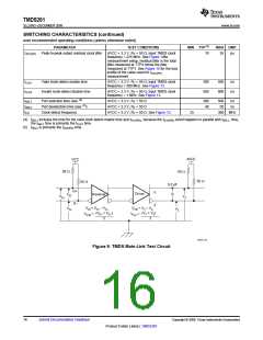
SWITCHING CHARACTERISTICS
over recommended operating conditions (unless otherwise noted)
PARAMETER
Propagation delay time, low to high
Propagation delay time, high to low
Propagation delay time, low to high
Propagation delay time, high to low
Output signal fall time
TEST CONDITIONS
Source to sink
Source to sink
Sink to source
Sink to source
Sink side
MIN
80
TYP
MAX UNIT
tPLH1
tPHL1
tPLH2
tPHL2
tf1
251
200
459
200
72
ns
ns
ns
ns
ns
ns
35
204
35
20
tf2
Output-signal fall time
Source side
Local I2C
Local I2C
Local I2C
Local I2C
Local I2C
Local I2C
Local I2C
Local I2C
20
72
fSCL
tW(L)
tW(H)
tSU1
th(1)
SCL clock frequency for internal register
Clock LOW period for I2C register
100 kHz
4.7
4
µs
µs
ns
µs
µs
µs
µs
µs
Clock HIGH period for internal register
Internal register setup time, SDA to SCL
Internal register hold time, SCL to SDA
Internal register bus free time between STOP and START
Internal register setup time, SCL to START
Internal register hold time, START to SCL
Internal register hold time, SCL to STOP
250
0
t(buf)
tsu(2)
th(2)
4.7
4.7
4
tsu(3)
Local I2C
4
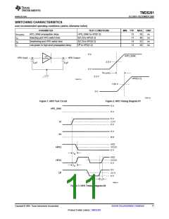
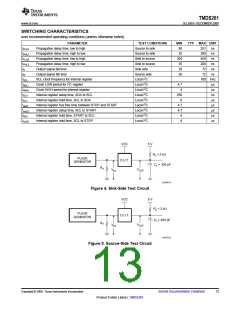
VCC
5 V
RL = 2 kW
PULSE
GENRATOR
D.U.T.
CL = 100 pF
RT
VOUT
VIN
S0369-02
Figure 4. Sink-Side Test Circuit
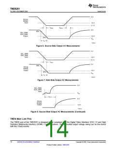
VCC
5 V
RL = 2 kW
PULSE
GENRATOR
D.U.T.
CL = 400 pF
RT
VOUT
VIN
S0370-02
Figure 5. Source-Side Test Circuit
Copyright © 2008, Texas Instruments Incorporated
Submit Documentation Feedback
13
Product Folder Link(s) :TMDS261

 TI [ TEXAS INSTRUMENTS ]