TLV3501-Q1
www.ti.com
SBOS533A –SEPTEMBER 2010–REVISED SEPTEMBER 2010
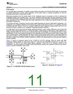
PCB Layout
For any high-speed comparator or amplifier, proper design and printed circuit board (PCB) layout are necessary
for optimal performance. Excess stray capacitance on the active input, or improper grounding, can limit the
maximum performance of high-speed circuitry.
Minimizing resistance from the signal source to the comparator input is necessary in order to minimize the
propagation delay of the complete circuit. The source resistance along with input and stray capacitance creates
an RC filter that delays voltage transitions at the input, and reduces the amplitude of high-frequency signals. The
input capacitance of the TLV350x along with stray capacitance from an input pin to ground results in several
picofarads of capacitance.
The location and type of capacitors used for power-supply bypassing are critical to high-speed comparators. The
suggested 2.2-mF tantalum capacitor do not need to be as close to the device as the 0.1-mF capacitor, and may
be shared with other devices. The 2.2-mF capacitor buffers the power-supply line against ripple, and the 0.1-mF
capacitor provides a charge for the comparator during high-frequency switching.
In a high-speed circuit, fast rising and falling switching transients create voltage differences across lines that
would be at the same potential at DC. To reduce this effect, a ground plane is often used to reduce difference in
voltage potential within the circuit board. A ground plane has the advantage of minimizing the effect of stray
capacitances on the circuit board by providing a more desirable path for the current to flow. With a signal trace
over a ground plane, at high-frequency the return current (in the ground plane) tends to flow right under the
signal trace. Breaks in the ground plane (as simple as through-hole leads and vias) increase the inductance of
the plane, making it less effective at higher frequencies. Breaks in the ground plane for necessary vias should be
spaced randomly.
Figure 21 shows an evaluation layout for the TLV3501-Q1 SOT23-6 package. Both are shown with SMA
connectors bringing signals on and off the board. RT1 and RT2 are termination resistors for +VIN and −VIN,
respectively. C1 and C2 are power-supply bypass capacitors. Place the 0.1-mF capacitor closest to the
comparator. The ground plane is not shown, but the pads that the resistors and capacitors connect to are shown.
Figure 22 shows a schematic of this circuit.
+VS
-VIN
SD
-VIN
C2
C1
100 nF
RT2
2.2 mF
50 W
VOUT
RT2
RT1
VOUT
TLV3501-Q1
+VIN
RT1
DUT
50 W
C1 C2
+VS
GND
Shutdown
+VIN
Figure 22. Schematic for Figure 21
Figure 21. TLV3501DBV (SOT23) Sample Layout
Copyright © 2010, Texas Instruments Incorporated
Submit Documentation Feedback
11
Product Folder Link(s): TLV3501-Q1

 TI [ TEXAS INSTRUMENTS ]