TL594
PULSE-WIDTH-MODULATION CONTROL CIRCUITS
SLVS052C – APRIL 1988 – REVISED JULY 1999
electrical characteristics over recommended operating free-air temperature range, V
(unless otherwise noted) (continued)
= 15 V,
CC
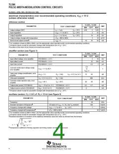
switching characteristics, T = 25°C
A
TL594C, TL594I
PARAMETER
TEST CONDITIONS
UNIT
†
MIN TYP
MAX
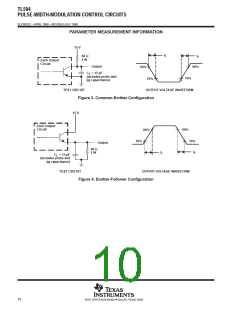
Output-voltage rise time
100
30
200
100
400
100
ns
ns
ns
ns
Common-emitter configuration (see Figure 3
Emitter-follower configuration (see Figure 4)
Output-voltage fall time
Output-voltage rise time
Output-voltage fall time
200
45
†
All typical values except for parameter changes with temperature are at T = 25°C.
A
electrical characteristics over recommended operating conditions, V
(unless otherwise noted)
= 15 V, T = 25°C
CC
A
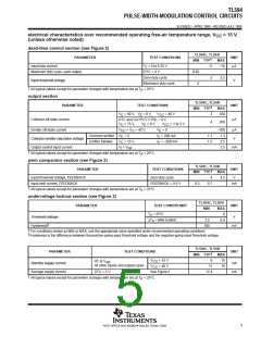
reference section
TL594Y
PARAMETER
TEST CONDITIONS
= 1 mA
UNIT
MIN
TYP
5
MAX
Output voltage (REF)
Input regulation
I
O
V
V
= 7 V to 40 V
2
mV
mV
mA
CC
= 1 to 10 mA
Output regulation
I
O
14
35
‡
Short-circuit output current
V
ref
= 0
‡
Duration of the short circuit should not exceed one second.
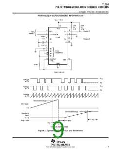
oscillator section, C = 0.01 µF, R = 12 kΩ (see Figure 2)
T
T
TL594Y
TYP
10
PARAMETER
TEST CONDITIONS
UNIT
MIN
MAX
Frequency
kHz
§
Standard deviation of frequency
Frequency change with voltage
All values of V , C , R , and T constant
100
1
Hz/kHz
Hz/kHz
CC
T
T
A
V
CC
= 7 V to 40 V
§
Standard deviation is a measure of the statistical distribution about the mean as derived from the formula:
N
2
X)
(x
n
n
1
N
1
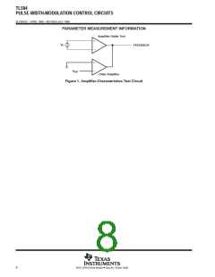
amplifier section (see Figure 1)
TL594Y
TYP
2
PARAMETER
TEST CONDITIONS
UNIT
MIN
MAX
Input offset voltage, error amplifier
Input offset current
FEEDBACK = 2.5 V
FEEDBACK = 2.5 V
FEEDBACK = 2.5 V
mV
nA
µA
25
Input bias current
0.2
Open-loop voltage amplification, error
amplifier
∆V = 3 V,
R
R
= 2 kΩ,
= 2 kΩ
= 25°C
V = 0.5 V to 3.5 V
O
95
800
80
dB
kHz
dB
O
L
L
Unity-gain bandwidth
V
V
V
= 0.5 V to 3.5 V,
O
Common-mode rejection ratio, error
amplifier
= 40 V,
T
A
CC
Output sink current, FEEDBACK
= –15 mV to –5 V,
FEEDBACK = 0.5 V
0.7
mA
ID
6
POST OFFICE BOX 655303 • DALLAS, TEXAS 75265

 TI [ TEXAS INSTRUMENTS ]