TAS5711
SLOS600 –DECEMBER 2009
www.ti.com
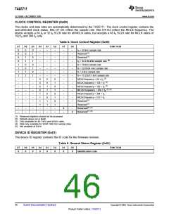
CLOCK CONTROL REGISTER (0x00)
The clocks and data rates are automatically determined by the TAS5711. The clock control register contains the
auto-detected clock status. Bits D7–D5 reflect the sample rate. Bits D4–D2 reflect the MCLK frequency. The
device accepts a 64 fS or 32 fS SCLK rate for all MCLK ratios, but accepts a 48 fS SCLK rate for MCLK ratios of
192 fS and 384 fS only.
Table 5. Clock Control Register (0x00)
D7
0
0
0
0
1
1
1
1
–
–
–
–
–
–
–
–
–
–
D6
0
0
1
1
0
0
1
1
–
–
–
–
–
–
–
–
–
–
D5
0
1
0
1
0
1
0
1
–
–
–
–
–
–
–
–
–
–
D4
–
–
–
–
–
–
–
–
0
0
0
0
1
1
1
1
–
–
D3
–
–
–
–
–
–
–
–
0
0
1
1
0
0
1
1
–
–
D2
–
–
–
–
–
–
–
–
0
1
0
1
0
1
0
1
–
–
D1
–
–
–
–
–
–
–
–
–
–
–
–
–
–
–
–
0
–
D0
–
–
–
–
–
–
–
–
–
–
–
–
–
–
–
–
–
0
FUNCTION
fS = 32-kHz sample rate
Reserved(1)
Reserved(1)
(2)
fS = 44.1/48-kHz sample rate
fs = 16-kHz sample rate
fs = 22.05/24 -kHz sample rate
fs = 8-kHz sample rate
fs = 11.025/12 -kHz sample rate
(3)
MCLK frequency = 64 × fS
(3)
MCLK frequency = 128 × fS
(4)
MCLK frequency = 192 × fS
(2) (5)
MCLK frequency = 256 × fS
MCLK frequency = 384 × fS
MCLK frequency = 512 × fS
Reserved(1)
Reserved(1)
Reserved(1) (2)
Reserved(1) (2)
(1) Reserved registers should not be accessed.
(2) Default values are in bold.
(3) Only available for 44.1 kHz and 48 kHz rates.
(4) Rate only available for 32/44.1/48 KHz sample rates
(5) Not available at 8 kHz
DEVICE ID REGISTER (0x01)
The device ID register contains the ID code for the firmware revision.
Table 6. General Status Register (0x01)
D7
0
D6
0
D5
0
D4
0
D3
0
D2
0
D1
0
D0
0
FUNCTION
Identification code
46
Submit Documentation Feedback
Copyright © 2009, Texas Instruments Incorporated
Product Folder Link(s): TAS5711

 TI [ TEXAS INSTRUMENTS ]