TAS5614LA
www.ti.com
SLAS846 –MAY 2012
CIRCUIT COMPONENT AND PRINTED CIRCUIT BOARD RECOMMENDATION
These requirements must be followed to achieve best performance and reliability and minimum ground bounce at
rated output power of TAS5614LA.
CIRCUIT COMPONENT REQUIREMENTS
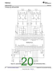
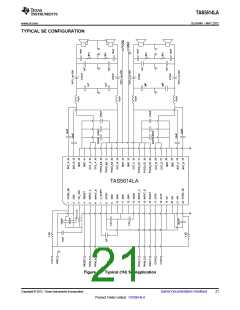
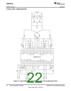
A number of circuit components are critical to performance and reliability. They include LC filter inductors and
capacitors, decoupling capacitors and the heatsink. The best detailed reference for these is the TAS5614LA
EVM BOM in the user's guide, which includes components that meet all the following requirements.
•
High frequency decoupling capacitors: small high frequency decoupling capacitors are placed next to the IC
to control switching spikes and keep high frequency currents in a tight loop to achieve best performance and
reliability and EMC. They must be high quality ceramic parts with material like X7R or X5R and voltage
ratings at least 30% greater than PVDD, to minimize loss of capacitance caused by applied DC voltage.
(Capacitors made of materials like Y5V or Z5U should never be used in decoupling circuits or audio circuits
because their capacitance falls dramatically with applied DC and AC voltage, often to 20% of rated value or
less.)
•
•
Bulk decoupling capacitors: large bulk decoupling capacitors are placed as close as possible to the IC to
stabilize the power supply at lower frequencies. They must be high quality aluminum parts with low ESR and
ESL and voltage ratings at least 25% more than PVDD to handle power supply ripple currents and voltages
LC filter inductors: to maintain high efficiency, short circuit protection and low distortion, LC filter inductors
must be linear to at least the OCP limit and must have low DC resistance and core losses. For SCP,
minimum working inductance, including all variations of tolerance, temperature and current level, must be
5µH. Inductance variation of more than 1% over the output current range can cause increased distortion.
•
•
LC filter capacitors: to maintain low distortion and reliable operation, LC filter capacitors must be linear to
twice the peak output voltage. For reliability, capacitors must be rated to handle the audio current generated
in them by the maximum expected audio output voltage at the highest audio frequency.
Heatsink:The heatsink must be fabricated with the PowerPad contact area spaced 1.0mm +/-0.01mm above
mounting areas that contact the PCB surface. It must be supported mechanically at each end of the IC. This
mounting ensures the correct pressure to provide good mechanical, thermal and electrical contact with
TAS5614LA PowerPAD. The PowerPAD contact area must be bare and must be interfaced to the PowerPAD
with a thin layer (about 1mil) of a thermal compound with high thermal conductivity.
PRINTED CIRCUIT BOARD REQUIREMENTS
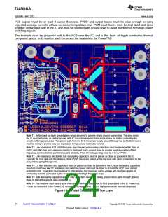
PCB layout, audio performance, EMC and reliability are linked closely together, and solid grounding improves
results in all these areas. The circuit produces high, fast-switching currents, and care must be taken to control
current flow and minimize voltage spikes and ground bounce at IC ground pins. Critical components must be
placed for best performance and PCB traces must be sized for the high audio currents that the IC circuit
produces.
Grounding: ground planes must be used to provide the lowest impedance and inductance for power and audio
signal currents between the IC and its decoupling capacitors, LC filters and power supply connection. The area
directly under the IC should be treated as central ground area for the device, and all IC grounds must be
connected directly to that area. A matrix of vias must be used to connect that area to the ground plane. Ground
planes can be interrupted by radial traces (traces pointing away from the IC), but they must never be interrupted
by circular traces, which disconnect copper outside the circular trace from copper between it and the IC. Top and
bottom areas that do not contain any power or signal traces should be flooded and connected with vias to the
ground plane.
Decoupling capacitors: high frequency decoupling capacitors must be located within 2mm of the IC and
connected directly to PVDD and GND pins with solid traces. Vias must not be used to complete these
connections, but several vias must be used at each capacitor location to connect top ground directly to the
ground plane. Placement of bulk decoupling capacitors is less critical, but they still must be placed as close as
possible to the IC with strong ground return paths. Typically the heatsink sets the distance.
LC filters: LC filters must be placed as close as possible to the IC after the decoupling capacitors. The capacitors
must have strong ground returns to the IC through top and bottom grounds for effective operation.
Copyright © 2012, Texas Instruments Incorporated
Submit Documentation Feedback
23
Product Folder Link(s): TAS5614LA

 TI [ TEXAS INSTRUMENTS ]