SN65176B, SN75176B
DIFFERENTIAL BUS TRANSCEIVERS
SLLS101D – JULY 1985 – REVISED APRIL 2003
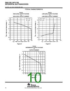
switching characteristics, V
= 5 V, C = 15 pF, T = 25°C
L A
CC
PARAMETER
TEST CONDITIONS
MIN
TYP
21
MAX
35
UNIT
t
t
t
t
t
t
Propagation delay time, low- to high-level output
Propagation delay time, high- to low-level output
Output enable time to high level
PLH
PHL
PZH
PZL
PHZ
PLZ
V
ID
= 0 to 3 V, See Figure 6
ns
23
35
10
20
See Figure 7
See Figure 7
ns
ns
Output enable time to low level
12
20
Output disable time from high level
Output disable time from low level
20
35
17
25
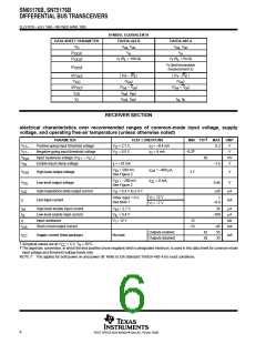
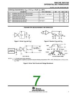
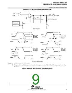
PARAMETER MEASUREMENT INFORMATION
V
ID
R
L
V
OH
2
V
OD2
+I
–I
OH
OL
R
V
OL
L
V
OC
2
Figure 1. Driver V
and V
Figure 2. Receiver V
and V
OL
OD
OC
OH
3 V
0 V
Input
1.5 V
1.5 V
C
= 50 pF
L
(see Note A)
t
t
d(OD)
d(OD)
R
= 54 Ω
L
Generator
(see Note B)
Output
50 Ω
≈2.5 V
90%
Output
50%
10%
50%
10%
≈–2.5 V
t(OD)
3 V
t
t
t(OD)
TEST CIRCUIT
VOLTAGE WAVEFORMS
NOTES: A.
C
includes probe and jig capacitance.
L
B. The input pulse is supplied by a generator having the following characteristics: PRR ≤ 1 MHz, 50% duty cycle, t ≤ 6 ns, t ≤ 6 ns,
r
f
Z
O
= 50 Ω.
Figure 3. Driver Test Circuit and Voltage Waveforms
7
POST OFFICE BOX 655303 • DALLAS, TEXAS 75265

 TI [ TEXAS INSTRUMENTS ]