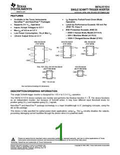
SN74LVC1G14
SINGLE SCHMITT-TRIGGER INVERTER
www.ti.com
SCES218S–APRIL 1999–REVISED SEPTEMBER 2005
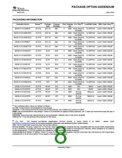
ORDERING INFORMATION
TA
PACKAGE(1)
ORDERABLE PART NUMBER TOP-SIDE MARKING(2)
NanoStar™ – WCSP (DSBGA)
0.17-mm Small Bump – YEA
SN74LVC1G14YEAR
NanoFree™ – WCSP (DSBGA)
0.17-mm Small Bump – YZA (Pb-free)
SN74LVC1G14YZAR
_ _ _CF_
Reel of 3000
Reel of 3000
NanoStar™ – WCSP (DSBGA)
0.23-mm Large Bump – YEP
SN74LVC1G14YEPR
NanoFree™ – WCSP (DSBGA)
0.23-mm Large Bump – YZP (Pb-free)
SN74LVC1G14YZPR
–40°C to 85°C
NanoFree™ – WCSP (DSBGA)
0.23-mm Large Bump – YZV (Pb-free)
_ _ _ _
SN74LVC1G14YZVR
CF
Reel of 3000
Reel of 250
Reel of 3000
Reel of 250
Reel of 4000
SN74LVC1G14DBVR
C14_
SOT (SOT-23) – DBV
SN74LVC1G14DBVT
SN74LVC1G14DCKR
CF_
SOT (SC-70) – DCK
SN74LVC1G14DCKT
SOT (SOT-553) – DRL
SN74LVC1G14DRLR
CF_
(1) Package drawings, standard packing quantities, thermal data, symbolization, and PCB design guidelines are available at
www.ti.com/sc/package.
(2) DBV/DCK/DRL: The actual top-side marking has one additional character that designates the assembly/test site.
YEA/YEP, YZA/YZP: The actual top-side marking has three preceding characters to denote year, month, and sequence code, and one
following character to designate the assembly/test site. Pin 1 identifier indicates solder-bump composition (1 = SnPb, • = Pb-free).
YZV: The actual top-side marking is on two lines. Line 1 has four characters to denote year, month, day, and assembly/test site. Line 2
has two characters which show the family and function code. Pin 1 identifier indicates solder-bump composition (1 = SnPb, • = Pb-free).
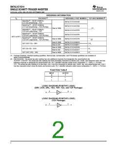
FUNCTION TABLE
INPUT
A
OUTPUT
Y
H
L
L
H
LOGIC DIAGRAM (POSITIVE LOGIC)
(DBV, DCK, DRL, YEA, YEP, YZA, and YZP Package)
2
4
A
Y
LOGIC DIAGRAM (POSITIVE LOGIC)
(YZV Package)
1
3
A
Y
2

 TI [ TEXAS INSTRUMENTS ]