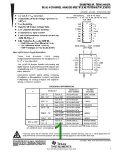
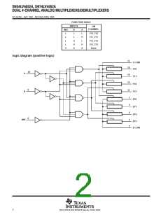
ꢀꢁ ꢂꢃ ꢄꢅꢃ ꢆ ꢂ ꢇ ꢈꢉ ꢀꢁ ꢊꢃ ꢄꢅ ꢃꢆ ꢂꢇ ꢈ
ꢋꢌ ꢈꢄ ꢃ ꢍꢎꢏꢈ ꢁꢁꢐꢄ ꢈꢁꢈ ꢄꢑ ꢒ ꢓ ꢌꢄꢔ ꢕꢖ ꢄꢐ ꢗꢐꢘꢀ ꢙꢋꢐ ꢓꢌ ꢄꢔ ꢕ ꢖꢄ ꢐꢗ ꢐ ꢘꢀ
SCLS429H − MAY 1999 − REVISED APRIL 2005
†
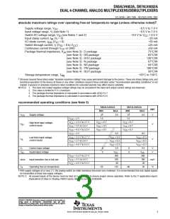
absolute maximum ratings over operating free-air temperature range (unless otherwise noted)
Supply voltage range, V
. . . . . . . . . . . . . . . . . . . . . . . . . . . . . . . . . . . . . . . . . . . . . . . . . . . . . . . . . −0.5 V to 7.0 V
CC
Input voltage range, V (see Note 1) . . . . . . . . . . . . . . . . . . . . . . . . . . . . . . . . . . . . . . . . . . . . . . . . . −0.5 V to 7.0 V
I
Switch I/O voltage range, V (see Notes 1 and 2) . . . . . . . . . . . . . . . . . . . . . . . . . . . . . . −0.5 V to V
+ 0.5 V
IO
CC
Input clamp current, I (V < 0) . . . . . . . . . . . . . . . . . . . . . . . . . . . . . . . . . . . . . . . . . . . . . . . . . . . . . . . . . . . −20 mA
IK
I
I/O diode current, I
(V < 0) . . . . . . . . . . . . . . . . . . . . . . . . . . . . . . . . . . . . . . . . . . . . . . . . . . . . . . . . . . −50 mA
IOK IO
Switch through current, I (V = 0 to V ) . . . . . . . . . . . . . . . . . . . . . . . . . . . . . . . . . . . . . . . . . . . . . . . . . 25 mA
T
IO
CC
CC
Continuous current through V
or GND . . . . . . . . . . . . . . . . . . . . . . . . . . . . . . . . . . . . . . . . . . . . . . . . . . . 50 mA
Package thermal impedance, θ (see Note 3): D package . . . . . . . . . . . . . . . . . . . . . . . . . . . . . . . . . . . 73°C/W
JA
(see Note 3): DB package . . . . . . . . . . . . . . . . . . . . . . . . . . . . . . . . . 82°C/W
(see Note 3): DGV package . . . . . . . . . . . . . . . . . . . . . . . . . . . . . . . 120°C/W
(see Note 3): N package . . . . . . . . . . . . . . . . . . . . . . . . . . . . . . . . . . . 67°C/W
(see Note 3): NS package . . . . . . . . . . . . . . . . . . . . . . . . . . . . . . . . . 64°C/W
(see Note 3): PW package . . . . . . . . . . . . . . . . . . . . . . . . . . . . . . . . 108°C/W
(see Note 4): RGY package . . . . . . . . . . . . . . . . . . . . . . . . . . . . . . . . 39°C/W
Storage temperature range, T
. . . . . . . . . . . . . . . . . . . . . . . . . . . . . . . . . . . . . . . . . . . . . . . . . . . −65°C to 150°C
stg
†
Stresses beyond those listed under “absolute maximum ratings” may cause permanent damage to the device. These are stress ratings only, and
functional operation of the device at these or any other conditions beyond those indicated under “recommended operating conditions” is not
implied. Exposure to absolute-maximum-rated conditions for extended periods may affect device reliability.
NOTES: 1. The input and output negative-voltage ratings may be exceeded if the input and output current ratings are observed.
2. This value is limited to 5.5 V maximum.
3. The package thermal impedance is calculated in accordance with JESD 51-7.
4. The package thermal impedance is calculated in accordance with JESD 51-5.
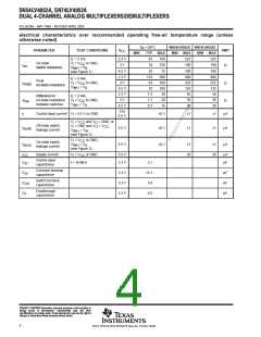
recommended operating conditions (see Note 5)
SN54LV4052A
MIN MAX
SN74LV4052A
MIN MAX
UNIT
‡
‡
V
V
Supply voltage
2
5.5
2
5.5
V
CC
V
CC
V
CC
V
CC
V
CC
V
CC
V
CC
V
CC
V
CC
= 2 V
1.5
1.5
= 2.3 V to 2.7 V
= 3 V to 3.6 V
= 4.5 V to 5.5 V
= 2 V
V
V
V
× 0.7
V
V
V
× 0.7
High-level input voltage,
control inputs
CC
CC
CC
CC
CC
CC
V
V
IH
× 0.7
× 0.7
× 0.7
× 0.7
0.5
0.5
= 2.3 V to 2.7 V
= 3 V to 3.6 V
= 4.5 V to 5.5 V
V
V
V
× 0.3
× 0.3
× 0.3
5.5
V
CC
V
CC
V
CC
× 0.3
× 0.3
× 0.3
5.5
Low-level input voltage,
control inputs
CC
CC
CC
V
IL
V
V
Control input voltage
Input/output voltage
0
0
0
0
V
V
I
V
V
CC
IO
CC
V
CC
V
CC
V
CC
= 2.3 V to 2.7 V
= 3 V to 3.6 V
= 4.5 V to 5.5 V
200
200
100
20
100
20
∆t/∆v
Input transition rise or fall rate
Operating free-air temperature
ns/V
T
A
−55
125
−40
85
°C
‡
With supply voltages at or near 2 V, the analog switch on-state resistance becomes very nonlinear. It is recommended that only digital signals
be transmitted at these low supply voltages.
NOTE 5: All unused inputs of the device must be held at V
or GND to ensure proper device operation. Refer to the TI application report,
Implications of Slow or Floating CMOS Inputs, literature number SCBA004.
CC
ꢖ
ꢘ
ꢑ
ꢋ
ꢌ
ꢎ
ꢔ
ꢖ
ꢘ
ꢐ
ꢅ
ꢕ
ꢐ
ꢚ
ꢝ
ꢥ
ꢧ
ꢠ
ꢨ
ꢣ
ꢦ
ꢛ
ꢝ
ꢠ
ꢥ
ꢡ
ꢠ
ꢥ
ꢡ
ꢤ
ꢨ
ꢥ
ꢞ
ꢩ
ꢨ
ꢠ
ꢟ
ꢢ
ꢟꢤ ꢞ ꢝ ꢰꢥ ꢩꢜ ꢦ ꢞ ꢤ ꢠꢧ ꢟꢤ ꢱ ꢤ ꢫꢠ ꢩꢣꢤ ꢥꢛꢬ ꢎ ꢜꢦ ꢨꢦ ꢡꢛ ꢤꢨ ꢝꢞ ꢛꢝ ꢡ ꢟꢦ ꢛꢦ ꢦꢥ ꢟ ꢠꢛ ꢜꢤꢨ
ꢡ
ꢛ
ꢞ
ꢝ
ꢥ
ꢛ
ꢜ
ꢤ
ꢧ
ꢠ
ꢨ
ꢣ
ꢦ
ꢛ
ꢝ
ꢱ
ꢤ
ꢠ
ꢨ
ꢞ
ꢩ
ꢤ
ꢡ
ꢝ
ꢧ
ꢝ
ꢡ
ꢦ
ꢛ
ꢝ
ꢠ
ꢥ
ꢞ
ꢦ
ꢨ
ꢤ
ꢟ
ꢤ
ꢞ
ꢝ
ꢰ
ꢥ
ꢰ
ꢠ
ꢦ
ꢫ
ꢞ
ꢬ
ꢔ
ꢤ
ꢭ
ꢦ
ꢞ
ꢕ
ꢥ
ꢞ
ꢛ
ꢨ
ꢢ
ꢣ
ꢤ
ꢥ
ꢡ ꢜꢦ ꢥ ꢰꢤ ꢠꢨ ꢟꢝ ꢞ ꢡ ꢠꢥ ꢛꢝ ꢥꢢꢤ ꢛ ꢜꢤ ꢞ ꢤ ꢩꢨ ꢠꢟ ꢢꢡꢛ ꢞ ꢮ ꢝꢛꢜ ꢠꢢꢛ ꢥꢠꢛ ꢝꢡꢤ ꢬ
ꢛ
ꢞ
ꢨ
ꢤ
ꢞ
ꢤ
ꢨ
ꢱ
ꢤ
ꢞ
ꢛ
ꢜ
ꢤ
ꢨ
ꢝ
ꢰ
ꢜ
ꢛ
ꢛ
ꢠ
3
POST OFFICE BOX 655303 • DALLAS, TEXAS 75265

 TI [ TEXAS INSTRUMENTS ]