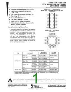
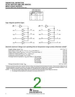
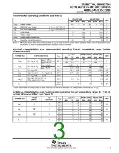
SN54HCT244, SN74HCT244
OCTAL BUFFERS AND LINE DRIVERS
WITH 3-STATE OUTPUTS
SCLS175D – MARCH 1984 – REVISED AUGUST 2003
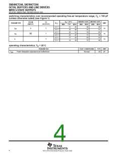
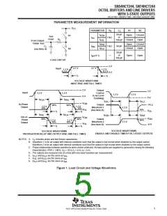
PARAMETER MEASUREMENT INFORMATION
V
CC
PARAMETER
R
C
S1
S2
L
L
50 pF
or
150 pF
t
Open
Closed
Closed
Open
S1
S2
PZH
Test
Point
t
t
1 kΩ
1 kΩ
en
R
t
t
t
L
PZL
PHZ
PLZ
From Output
Under Test
Open
Closed
Open
50 pF
C
dis
L
Closed
(see Note A)
50 pF
or
150 pF
t
or t
––
Open
Open
pd
t
LOAD CIRCUIT
Input
3 V
2.7 V
2.7 V
1.3 V
0.3 V
1.3 V
0.3 V
0 V
t
t
r
f
VOLTAGE WAVEFORM
INPUT RISE AND FALL TIMES
3 V
0 V
Output
3 V
0 V
Input
Control
(Low-Level
Enabling)
1.3 V
1.3 V
1.3 V
1.3 V
t
t
PLH
PHL
90%
t
t
PLZ
PZL
V
V
OH
In-Phase
Output
≈V
CC
Output
Waveform 1
(See Note B)
90%
t
1.3 V
10%
1.3 V
10%
1.3 V
10%
t
OL
V
OL
OH
t
r
f
f
t
t
t
PHL
90%
PLH
PZH
PHZ
Out-of-
Phase
Output
V
V
OH
V
90%
t
Output
Waveform 2
(See Note B)
90%
1.3 V
10%
1.3 V
10%
1.3 V
OL
≈0 V
t
r
VOLTAGE WAVEFORMS
ENABLE AND DISABLE TIMES FOR 3-STATE OUTPUTS
VOLTAGE WAVEFORMS
PROPAGATION DELAY AND OUTPUT RISE AND FALL TIMES
NOTES: A.
C includes probe and test-fixture capacitance.
L
B. Waveform 1 is for an output with internal conditions such that the output is low except when disabled by the output control.
Waveform 2 is for an output with internal conditions such that the output is high except when disabled by the output control.
C. Phase relationships between waveforms were chosen arbitrarily. All input pulses are supplied by generators having the following
characteristics: PRR ≤ 1 MHz, Z = 50 Ω, t = 6 ns, t = 6 ns.
O
r
f
D. The outputs are measured one at a time with one input transition per measurement.
E.
F.
G.
t
t
t
and t
and t
and t
are the same as t
are the same as t
are the same as t
.
dis
en
.
pd
PLZ
PZL
PLH
PHZ
PZH
PHL
.
Figure 1. Load Circuit and Voltage Waveforms
5
POST OFFICE BOX 655303 • DALLAS, TEXAS 75265

 TI [ TEXAS INSTRUMENTS ]