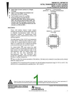
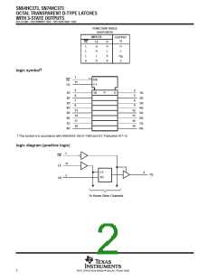
SN54HC373, SN74HC373
OCTAL TRANSPARENT D-TYPE LATCHES
WITH 3-STATE OUTPUTS
SCLS140B – DECEMBER 1982 – REVISED MAY 1997
†
absolute maximum ratings over operating free-air temperature range
Supply voltage range, V
. . . . . . . . . . . . . . . . . . . . . . . . . . . . . . . . . . . . . . . . . . . . . . . . . . . . . . . . . . –0.5 V to 7 V
CC
I
Input clamp current, I (V < 0 or V > V ) (see Note 1) . . . . . . . . . . . . . . . . . . . . . . . . . . . . . . . . . . . . ±20 mA
IK
I
CC
Output clamp current, I
(V < 0 or V > V ) (see Note 1) . . . . . . . . . . . . . . . . . . . . . . . . . . . . . . . . ±20 mA
OK
O O CC
Continuous output current, I (V = 0 to V ) . . . . . . . . . . . . . . . . . . . . . . . . . . . . . . . . . . . . . . . . . . . . . . ±35 mA
Continuous current through V
Package thermal impedance, θ (see Note 2): DB package . . . . . . . . . . . . . . . . . . . . . . . . . . . . . . . . 115°C/W
O
O
CC
CC
or GND . . . . . . . . . . . . . . . . . . . . . . . . . . . . . . . . . . . . . . . . . . . . . . . . . . . ±70 mA
JA
DW package . . . . . . . . . . . . . . . . . . . . . . . . . . . . . . . . . 97°C/W
N package . . . . . . . . . . . . . . . . . . . . . . . . . . . . . . . . . . . 67°C/W
PW package . . . . . . . . . . . . . . . . . . . . . . . . . . . . . . . . 128°C/W
Storage temperature range, T
. . . . . . . . . . . . . . . . . . . . . . . . . . . . . . . . . . . . . . . . . . . . . . . . . . . –65°C to 150°C
stg
†
Stresses beyond those listed under “absolute maximum ratings” may cause permanent damage to the device. These are stress ratings only, and
functional operation of the device at these or any other conditions beyond those indicated under “recommended operating conditions” is not
implied. Exposure to absolute-maximum-rated conditions for extended periods may affect device reliability.
NOTES: 1. The input and output voltage ratings may be exceeded if the input and output current ratings are observed.
2. The package thermal impedance is calculated in accordance with JESD 51, except for through-hole packages, which use a trace
length of zero.
recommended operating conditions
SN54HC373
MIN NOM
SN74HC373
MIN NOM
UNIT
MAX
MAX
V
V
Supply voltage
2
1.5
3.15
4.2
0
5
6
2
1.5
3.15
4.2
0
5
6
V
CC
V
CC
V
CC
V
CC
V
CC
V
CC
V
CC
= 2 V
High-level input voltage
= 4.5 V
= 6 V
V
V
IH
= 2 V
0.5
1.35
1.8
0.5
1.35
1.8
V
IL
Low-level input voltage
= 4.5 V
= 6 V
0
0
0
0
V
V
Input voltage
0
V
V
0
V
V
V
V
I
CC
CC
Output voltage
0
0
O
CC
CC
V
CC
V
CC
V
CC
= 2 V
0
1000
500
400
125
0
1000
500
400
85
t
Input transition (rise and fall) time
Operating free-air temperature
= 4.5 V
= 6 V
0
0
ns
t
0
0
T
–55
–40
°C
A
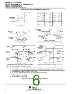
3
POST OFFICE BOX 655303 • DALLAS, TEXAS 75265

 TI [ TEXAS INSTRUMENTS ]