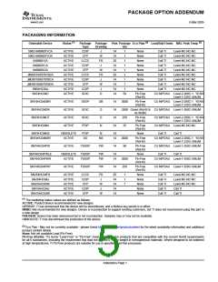
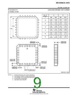
SN54HC04, SN74HC04
HEX INVERTERS
SCLS078D – DECEMBER 1982 – REVISED JULY 2003
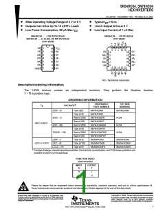
logic diagram (positive logic)
A
Y
†
absolute maximum ratings over operating free-air temperature range (unless otherwise noted)
Supply voltage range, V
. . . . . . . . . . . . . . . . . . . . . . . . . . . . . . . . . . . . . . . . . . . . . . . . . . . . . . . . . . –0.5 V to 7 V
CC
I
Input clamp current, I (V < 0 or V > V ) (see Note 1) . . . . . . . . . . . . . . . . . . . . . . . . . . . . . . . . . . . . ±20 mA
IK
I
CC
Output clamp current, I
(V < 0 or V > V ) (see Note 1) . . . . . . . . . . . . . . . . . . . . . . . . . . . . . . . . ±20 mA
OK
O O CC
Continuous output current, I (V = 0 to V ) . . . . . . . . . . . . . . . . . . . . . . . . . . . . . . . . . . . . . . . . . . . . . . ±25 mA
Continuous current through V
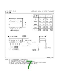
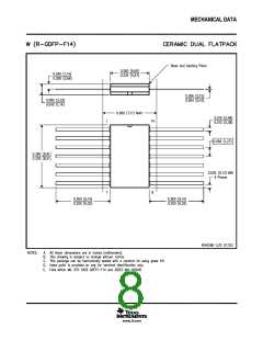
Package thermal impedance, θ (see Note 2): D package . . . . . . . . . . . . . . . . . . . . . . . . . . . . . . . . . . . 86°C/W
O
O
CC
CC
or GND . . . . . . . . . . . . . . . . . . . . . . . . . . . . . . . . . . . . . . . . . . . . . . . . . . . ±50 mA
JA
N package . . . . . . . . . . . . . . . . . . . . . . . . . . . . . . . . . . . 80°C/W
NS package . . . . . . . . . . . . . . . . . . . . . . . . . . . . . . . . . 76°C/W
PW package . . . . . . . . . . . . . . . . . . . . . . . . . . . . . . . . 113°C/W
Storage temperature range, T
. . . . . . . . . . . . . . . . . . . . . . . . . . . . . . . . . . . . . . . . . . . . . . . . . . . –65°C to 150°C
stg
†
Stresses beyond those listed under “absolute maximum ratings” may cause permanent damage to the device. These are stress ratings only, and
functional operation of the device at these or any other conditions beyond those indicated under “recommended operating conditions” is not
implied. Exposure to absolute-maximum-rated conditions for extended periods may affect device reliability.
NOTES: 1. The input and output voltage ratings may be exceeded if the input and output current ratings are observed.
2. The package thermal impedance is calculated in accordance with JESD 51-7.
recommended operating conditions (see Note 3)
SN54HC04
SN74HC04
MIN NOM
UNIT
MIN NOM
MAX
MAX
V
V
Supply voltage
2
1.5
5
6
2
1.5
5
6
V
CC
V
CC
V
CC
V
CC
V
CC
V
CC
V
CC
= 2 V
High-level input voltage
= 4.5 V
= 6 V
3.15
4.2
3.15
4.2
V
V
IH
= 2 V
0.5
1.35
1.8
0.5
1.35
1.8
V
IL
Low-level input voltage
= 4.5 V
= 6 V
V
V
Input voltage
0
0
V
V
0
0
V
V
V
V
I
CC
CC
Output voltage
O
CC
CC
V
CC
V
CC
V
CC
= 2 V
1000
500
400
125
1000
500
400
85
∆t/∆v
Input transition rise/fall time
= 4.5 V
= 6 V
ns
T
A
Operating free-air temperature
–55
–40
°C
NOTE 3: All unused inputs of the device must be held at V
or GND to ensure proper device operation. Refer to the TI application report,
CC
Implications of Slow or Floating CMOS Inputs, literature number SCBA004.
2
POST OFFICE BOX 655303 • DALLAS, TEXAS 75265

 TI [ TEXAS INSTRUMENTS ]