SN54AHCT32, SN74AHCT32
QUADRUPLE 2-INPUT POSITIVE-OR GATES
SCLS248L – OCTOBER 1995 – REVISED JULY 2003
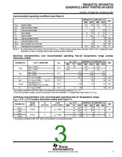
recommended operating conditions (see Note 4)
SN54AHCT32 SN74AHCT32
UNIT
MIN
4.5
2
MAX
MIN
4.5
2
MAX
V
V
V
V
V
Supply voltage
5.5
5.5
V
V
CC
IH
IL
High-level input voltage
Low-level input voltage
Input voltage
0.8
5.5
0.8
5.5
V
0
0
0
0
V
I
Output voltage
V
CC
V
CC
V
O
I
High-level output current
Low-level output current
Input transition rise or fall rate
Operating free-air temperature
–8
–8
mA
mA
ns/V
°C
OH
OL
I
8
8
20
85
∆t/∆v
20
T
–55
125
–40
A
NOTE 4: All unused inputs of the device must be held at V
or GND to ensure proper device operation. Refer to the TI application report,
CC
Implications of Slow or Floating CMOS Inputs, literature number SCBA004.
electrical characteristics over recommended operating free-air temperature range (unless
otherwise noted)
T
A
= 25°C
TYP
SN54AHCT32 SN74AHCT32
PARAMETER
TEST CONDITIONS
= –50
V
UNIT
V
CC
MIN
4.4
MAX
MIN
4.4
MAX
MIN
4.4
MAX
I
I
I
I
A
4.5
OH
OH
OL
OL
V
4.5 V
4.5 V
OH
OL
= –8 mA
= 50
= 8 mA
3.94
3.8
3.8
A
0.1
0.36
±0.1
2
0.1
0.44
±1*
20
0.1
0.44
±1
V
V
I
I
V = 5.5 V or GND
0 V to 5.5 V
5.5 V
A
A
I
I
V = V
or GND,
I = 0
O
20
CC
I
CC
One input at 3.4 V,
Other inputs at V
†
5.5 V
5 V
1.35
1.5
1.5
10
mA
pF
∆I
CC
or GND
CC
V = V or GND
CC
C
2
10
i
I
* On products compliant to MIL-PRF-38535, this parameter is not production tested at V
CC
= 0 V.
†
This is the increase in supply current for each input at one of the specified TTL voltage levels, rather than 0 V or V
CC
.
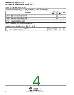
switching characteristics over recommended operating free-air temperature range,
V
= 5 V ± 0.5 V (unless otherwise noted) (see Figure 1)
CC
T
A
= 25°C
TYP
5**
SN54AHCT32 SN74AHCT32
FROM
(INPUT)
TO
(OUTPUT)
LOAD
CAPACITANCE
PARAMETER
UNIT
ns
MIN
MAX
6.9**
6.9**
7.9
MIN
1**
1**
1
MAX
8**
8**
9
MIN
1
MAX
t
t
t
t
8
8
9
9
PLH
PHL
PLH
PHL
A or B
A or B
Y
Y
C
C
= 15 pF
= 50 pF
L
L
5**
1
5.5
1
ns
5.5
7.9
1
9
1
** On products compliant to MIL-PRF-38535, this parameter is not production tested.
3
POST OFFICE BOX 655303 • DALLAS, TEXAS 75265

 TI [ TEXAS INSTRUMENTS ]