ꢀꢁ ꢂꢃ ꢄ ꢅꢆꢇ ꢈ ꢉ ꢊ ꢀꢁ ꢋꢃ ꢄꢅ ꢆꢇ ꢈꢉ
ꢌꢍ ꢎꢎ ꢏꢐ ꢏꢁꢑ ꢍꢒ ꢄ ꢑ ꢐꢒꢁ ꢀꢆ ꢏ ꢍꢓ ꢏ ꢐ
ꢔ ꢍꢑ ꢕ ꢑ ꢐꢒꢁꢀ ꢍꢏꢁ ꢑ ꢓꢖ ꢄꢑꢒꢗ ꢏ ꢀꢘ ꢙꢙꢐ ꢏꢀ ꢀ ꢍꢖ ꢁ
ꢚ
www.DataSheet4U.com
SLLS236F − OCTOBER 1996 − REVISED APRIL 2005
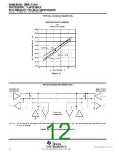
APPLICATION INFORMATION
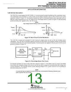
’LBC184 test description
The ’LBC184 is tested against the IEC 61000−4−5 recommended transient identified as the combination wave.
The combination wave provides a 1.2-/50-µs open-circuit voltage waveform and a 8-/20-µs short-circuit current
waveform shown in Figure 15. The testing is performed with a combination/hybrid pulse generator with an
effective output impedance of 2 Ω. The setup for the overvoltage stress is shown in Figure 16 with all testing
performed with power applied to the ’LBC184 circuit.
NOTE
High voltage transient testing is done on a sampling basis.
V
I
I(peak)
I(peak)
0.5 V
0.5 I
P
P
1.2 µs
8 µs
t
t
50 µs
20 µs
Figure 15. Short-Circuit Current Waveforms
The ’LBC184 is tested and evaluated for both maximum (single pulse) as well as life test (multiple pulse)
capabilities. The ’LBC184 is evaluated against transients of both positive and negative polarity and all testing
is performed with the worst-case transient polarity. Transient pulses are applied to the bus pins (A & B) across
ground as shown in Figure 16.
I
P
41.9 Ω
High
Low
7
5
Key Tech
1.2/50 − 8/20
Combination Pulse
Generator
B/A
SN75LBC184
3 Ω
V
P
GND
Current
Limiter
2-Ω Internal Impedance
Figure 16. Overvoltage-Stress Test Circuit
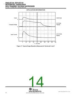
An example waveform as seen by the ’LBC184 is shown in Figure 17. The bottom trace is current, the middle
trace shows the clamping voltage of the device and the top trace is power as calculated from the voltage and
current waveforms. This example shows a peak clamping voltage of 16 V, peak current of 33.6 A yielding an
absorbed peak power of 538 W.
NOTE
A circuit reset may be required to ensure normal data communications following a transient noise
pulse of greater than 250 W peak.
13
POST OFFICE BOX 655303 • DALLAS, TEXAS 75265

 TI [ TEXAS INSTRUMENTS ]