SN54AHC132, SN74AHC132
QUADRUPLE POSITIVE-NAND GATES
WITH SCHMITT-TRIGGER INPUTS
SCLS365G – MAY 1997 – REVISED SEPTEMBER 2002
description/ordering information (continued)
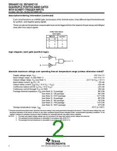
Each circuit functions as a NAND gate, but because of the Schmitt action, it has different input threshold levels
for positive- and negative-going signals.
These circuits are temperature compensated and can be triggered from the slowest of input ramps and still give
clean jitter-free output signals.
FUNCTION TABLE
(each gate)
INPUTS
OUTPUT
Y
A
B
H
X
L
H
L
L
H
H
X
logic diagram, each gate (positive logic)
A
Y
B
†
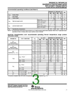
absolute maximum ratings over operating free-air temperature range (unless otherwise noted)
Supply voltage range, V
. . . . . . . . . . . . . . . . . . . . . . . . . . . . . . . . . . . . . . . . . . . . . . . . . . . . . . . . . . –0.5 V to 7 V
CC
Input voltage range, V (see Note 1) . . . . . . . . . . . . . . . . . . . . . . . . . . . . . . . . . . . . . . . . . . . . . . . . . . –0.5 V to 7 V
I
Output voltage range, V (see Note 1) . . . . . . . . . . . . . . . . . . . . . . . . . . . . . . . . . . . . . . . . –0.5 V to V
+ 0.5 V
O
CC
Input clamp current, I (V < 0) . . . . . . . . . . . . . . . . . . . . . . . . . . . . . . . . . . . . . . . . . . . . . . . . . . . . . . . . . . . –20 mA
IK
I
Output clamp current, I
(V < 0 or V > V ) . . . . . . . . . . . . . . . . . . . . . . . . . . . . . . . . . . . . . . . . . . . . ±20 mA
OK
O O CC
Continuous output current, I (V = 0 to V ) . . . . . . . . . . . . . . . . . . . . . . . . . . . . . . . . . . . . . . . . . . . . . . ±25 mA
Continuous current through V
Package thermal impedance, θ (see Note 2): D package . . . . . . . . . . . . . . . . . . . . . . . . . . . . . . . . . . . 86°C/W
O
O
CC
CC
or GND . . . . . . . . . . . . . . . . . . . . . . . . . . . . . . . . . . . . . . . . . . . . . . . . . . . ±50 mA
JA
(see Note 2): DB package . . . . . . . . . . . . . . . . . . . . . . . . . . . . . . . . . 96°C/W
(see Note 2): DGV package . . . . . . . . . . . . . . . . . . . . . . . . . . . . . . . 127°C/W
(see Note 2): N package . . . . . . . . . . . . . . . . . . . . . . . . . . . . . . . . . . . 80°C/W
(see Note 2): NS package . . . . . . . . . . . . . . . . . . . . . . . . . . . . . . . . . 76°C/W
(see Note 2): PW package . . . . . . . . . . . . . . . . . . . . . . . . . . . . . . . . 113°C/W
(see Note 3): RGY package . . . . . . . . . . . . . . . . . . . . . . . . . . . . . . . . 47°C/W
Storage temperature range, T
. . . . . . . . . . . . . . . . . . . . . . . . . . . . . . . . . . . . . . . . . . . . . . . . . . . –65°C to 150°C
stg
†
Stresses beyond those listed under “absolute maximum ratings” may cause permanent damage to the device. These are stress ratings only, and
functional operation of the device at these or any other conditions beyond those indicated under “recommended operating conditions” is not
implied. Exposure to absolute-maximum-rated conditions for extended periods may affect device reliability.
NOTES: 1. The input and output voltage ratings may be exceeded if the input and output current ratings are observed.
2. The package thermal impedance is calculated in accordance with JESD 51-7.
3. The package thermal impedance is calculated in accordance with JESD 51-5.
2
POST OFFICE BOX 655303 • DALLAS, TEXAS 75265

 TI [ TEXAS INSTRUMENTS ]