ꢀ
ꢁ
ꢂ
ꢃ
ꢄ
ꢅ
ꢆ
www.ti.com
SLES080B – MAY 2003 – REVISED NOVEMBER 2003
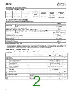
ORDERING INFORMATION
OPERATION
TEMPERATURE
RANGE
PACKAGE
MARKING
ORDERING
NUMBER
TRANSPORT
MEDIA
PRODUCT
PACKAGE
PACKAGE CODE
PCM1794DB
Tube
PCM1794DB
28-lead SSOP
28DB
–25°C to 85°C
PCM1794
PCM1794DBR
Tape and reel
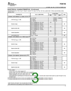
ABSOLUTE MAXIMUM RATINGS
(1)
over operating free-air temperature range unless otherwise noted
PCM1794
V
V
1, V 2L, V 2R
CC CC
–0.3 V to 6.5 V
–0.3 V to 4 V
0.1 V
CC
DD
Supply voltage
Supply voltage differences: V 1, V 2L, V 2R
CC CC CC
Ground voltage differences: AGND1, AGND2, AGND3L, AGND3R, DGND
0.1 V
LRCK, DATA, BCK, SCK, FMT1, FMT0, MONO, CHSL, DEM, MUTE, RST,
ZERO
–0.3 V to 6.5 V
Digital input voltage
Analog input voltage
–0.3 V to (V
+ 0.3 V) < 4 V
DD
–0.3 V to (V
+ 0.3 V) < 6.5 V
CC
Input current (any pins except supplies)
Ambient temperature under bias
Storage temperature
10 mA
–40°C to 125°C
–55°C to 150°C
150°C
Junction temperature
Lead temperature (soldering)
Package temperature (IR reflow, peak)
260°C, 5 s
250°C
(1)
Stresses beyond those listed under “absolute maximum ratings” may cause permanent damage to the device. These are stress ratings only, and
functional operation of the device at these or any other conditions beyond those indicated under “recommended operating conditions” is not
implied. Exposure to absolute-maximum-rated conditions for extended periods may affect device reliability.
ELECTRICAL CHARACTERISTICS
all specifications at T = 25°C, V 1 = V 2L = V 2R = 5 V, V
= 3.3 V, f = 44.1 kHz, system clock = 256 f , and 24-bit data, unless
A
CC
CC
CC
DD
S
S
otherwise noted
PCM1794DB
PARAMETER
TEST CONDITIONS
UNIT
MIN
TYP
MAX
RESOLUTION
DATA FORMAT
24
Bits
2
Audio data interface format
Audio data bit length
Audio data format
Standard, I S, left justified
16-, 24-bit selectable
MSB first, 2s complement
f
S
Sampling frequency
System clock frequency
10
200
kHz
128, 192, 256, 384, 512, 768 f
S
DIGITAL INPUT/OUTPUT
Logic family
TTL compatible
V
V
2
IH
IL
Input logic level
Input logic current
Output logic level
VDC
µA
0.8
10
I
IH
I
IL
V
V
= V
DD
= 0 V
IN
IN
–10
2.4
0.4
V
I
= –2 mA
= 2 mA
OH
OL
OH
OL
VDC
V
I
2

 TI [ TEXAS INSTRUMENTS ]