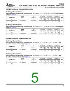
PCA9306
DUAL BIDIRECTIONAL I2C BUS AND SMBus VOLTAGE-LEVEL TRANSLATOR
www.ti.com
SCPS113–OCTOBER 2004–REVISED APRIL 2005
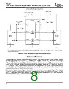
APPLICATION INFORMATION
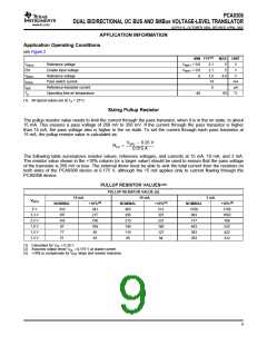
Application Operating Conditions
see Figure 2
MIN TYP(1)
MAX UNIT
VREF2
EN
Reference voltage
VREF1 + 0.6
2.1
2.1
1.5
14
5
5
5
V
V
Enable input voltage
VREF1 + 0.6
0
VREF1
IPASS
IREF
TA
Reference voltage
4.4
V
Pass switch current
mA
µA
°C
Reference-transistor current
Operating free-air temperature
–40
85
(1) All typical values are at TA = 25°C.
Sizing Pullup Resistor
The pullup resistor value needs to limit the current through the pass transistor, when it is in the on state, to about
15 mA. This ensures a pass voltage of 260 mV to 350 mV. If the current through the pass transistor is higher
than 15 mA, the pass voltage also is higher in the on state. To set the current through each pass transistor at
15 mA, the pullup resistor value is calculated as:
VDPU 0.35 V
RPU
+
0.015 A
The following table summarizes resistor values, reference voltages, and currents at 15 mA, 10 mA, and 3 mA.
The resistor value shown in the +10% column (or a larger value) should be used to ensure that the pass voltage
of the transistor is 350 mV or less. The external driver must be able to sink the total current from the resistors on
both sides of the PCA9306 device at 0.175 V, although the 15 mA applies only to current flowing through the
PCA9306 device.
(1)(2)
PULLUP RESISTOR VALUES
PULLUP RESISTOR VALUE (Ω)
15 mA
10 mA
3 mA
VDPU
NOMINAL
310
+10%(3)
341
217
158
106
85
NOMINAL
465
+10%(3)
512
NOMINAL
1550
983
+10%(3)
1705
1082
788
5 V
3.3 V
2.5 V
1.8 V
1.5 V
1.2 V
197
295
325
143
215
237
717
97
145
160
483
532
77
115
127
383
422
57
63
85
94
283
312
(1) Calculated for VOL = 0.35 V
(2) Assumes output driver VOL = 0.175 V at stated current
(3) +10% to compensate for VDD range and resistor tolerance
9

 TI [ TEXAS INSTRUMENTS ]