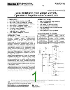
www.ti.com
ꢂ ꢀꢉ ꢠꢡꢢ ꢣ
SBOS249D − JUNE 2003− REVISED APRIL 2004
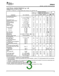
ELECTRICAL CHARACTERISTICS: V = 6V
S
Boldface limits are tested at +25°C.
R = 402Ω, R = 100Ω, and G = +2, unless otherwise noted. See Figure 1 for AC performance only.
F
L
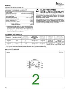
OPA2613ID, OPA2613IDTJ
MIN/MAX OVER TEMPERATURE
TYP
TEST
0°C to
−40°C to
MIN/
MAX
LEVEL
(1)
(2)
(2)
(3)
PARAMETER
TEST CONDITIONS
+25°C
+25°C
+70°C
+85°C
UNITS
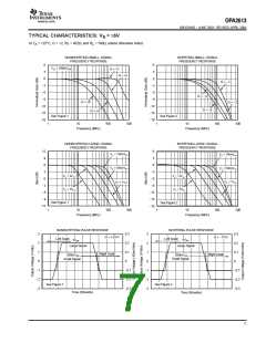
AC Performance (see Figure 1)
Small-Signal Bandwidth
G = +1, V = 0.1V , R = 0Ω
230
110
13
125
5
MHz
MHz
MHz
MHz
MHz
dB
typ
min
min
min
typ
typ
typ
min
typ
typ
typ
C
B
B
B
C
C
C
B
C
C
C
O
PP
F
G = +2, V = 0.1V
80
10
95
75
9
70
9
O
PP
G = +10, V = 0.1V
O
PP
Gain-Bandwidth Product
Bandwidth for 0.1dB Gain Flatness
Peaking at a Gain of +1
Large-Signal Bandwidth
Slew Rate
G ≥ 20
80
75
G = +2, V < 0.1V
O
PP
V
< 0.1V
1
O
PP
G = +2, V = 2V
22
70
3.6
55
40
MHz
V/µs
ns
O
PP
G = +2, 4V step
56
4.8
68
51
51
5.4
71
53
50
5.5
72
54
Rise-and-Fall Time
Settling Time to 0.02%
0.1%
G = +2, V = 0.2V Step
O
G = +2, V = 2V Step
ns
O
G = +2, V = 2V Step
ns
O
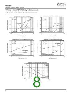
Harmonic Distortion
2nd-Harmonic
G = +2, f = 1MHz, V = 2V
O
PP
R
= 20Ω
≥ 500Ω
= 20Ω
−70
−95
−84
−97
1.8
−63
−90
−80
−92
2.0
−61
−88
−78
−90
2.1
−60
−87
−77
−89
2.3
dBc
dBc
max
max
max
max
max
max
typ
B
B
B
B
B
B
C
C
C
L
R
L
3rd-Harmonic
R
dBc
L
R
≥ 500Ω
dBc
L
Input Voltage Noise
Input Current Noise
Differential Gain
f > 10kHz
nV/√Hz
pA/√Hz
%
f > 10kHz
1.7
2.1
2.2
2.4
G = +2, PAL, V = 1.4V , R = 150Ω
0.02
0.03
−80
O
P
L
Differential Phase
G = +2, PAL, V = 1.4V , R = 150Ω
deg
typ
O
P
L
Channel-to-Channel Crosstalk
f = 1MHz, Input Referred
dBc
typ
(4)
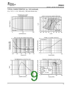
DC Performance
Open-Loop Gain (A
)
V
= 0V, R = 100Ω
97
92
92
1.15
3.3
−13
−30
520
5
91
1.2
dB
mV
min
max
max
max
max
max
max
A
A
B
A
B
A
B
OL
Input Offset Voltage
O
L
V
V
V
V
V
V
= 0V
= 0V
= 0V
= 0V
= 0V
= 0V
0.2
1.0
CM
CM
CM
CM
CM
CM
Average Offset Voltage Drift
Input Bias Current
3.3
µV/°C
µA
nA/°C
nA
−6
50
−12
300
−14.5
−35
750
7
Average Bias Current Drift (Magnitude)
Input Offset Current
Average Offset Bias Current Drift
nA/°C
Input
(5)
Common-Mode Input Range (CMIR)
4.7
4.5
88
4.5
87
4.4
86
V
min
min
A
A
Common-Mode Rejection Ratio (CMRR)
Input Impedance
V
=
1V
= 0
100
dB
CM
Differential-Mode
V
V
18 0.6
7 1
kΩ pF
MΩ pF
typ
typ
C
C
CM
CM
Common-Mode
= 0
Output
Output Voltage Swing
No Load
5.0
4.9
4.8
4.7
4.8
4.7
4.7
4.6
V
V
min
min
min
min
typ
A
A
A
A
C
C
100Ω
= 0, Linear Operation
Current Output, Sourcing
Current Output, Sinking
Short-Circuit Current
V
V
+350
−350
500
+280
−280
+240
−240
+220
−220
mA
mA
mA
Ω
O
= 0, Linear Operation
O
Output Shorted to Ground
G = +2, f = 100kHz
Closed-Loop Output Impedance
0.01
typ
(1)
(2)
Junction temperature = ambient for +25°C tested specifications.
Junction temperature = ambient at low temperature limit; junction temperature = ambient +23°C at high temperature limit for over temperature
tested specifications.
Test levels: (A) 100% tested at +25°C. Over temperature limits by characterization and simulation. (B) Limits set by characterization and
simulation.(C) Typical value only for information.
(3)
(4)
(5)
(6)
Current is considered positive-out-of-node. V
CM
is the input common-mode voltage.
Tested < 3dB below minimum CMRR specification at CMIR limits.
Heat slug soldered to heat spreading plane. This plane should be electrically floating or at V voltage.
−
S
3

 TI [ TEXAS INSTRUMENTS ]