OPA140
OPA2140, OPA4140
SBOS498A –JULY 2010–REVISED AUGUST 2010
www.ti.com
This integrated circuit can be damaged by ESD. Texas Instruments recommends that all integrated circuits be handled with
appropriate precautions. Failure to observe proper handling and installation procedures can cause damage.
ESD damage can range from subtle performance degradation to complete device failure. Precision integrated circuits may be more
susceptible to damage because very small parametric changes could cause the device not to meet its published specifications.
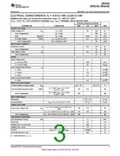
ABSOLUTE MAXIMUM RATINGS(1)
Over operating free-air temperature range (unless otherwise noted).
VALUE
UNIT
V
Supply Voltage
±20
(V–) –0.5 to (V+) +0.5
±10
Voltage(2)
Current(2)
V
Signal Input
Terminals
mA
Output Short-Circuit(3)
Continuous
Operating Temperature, TA
Storage Temperature, TA
Junction Temperature, TJ
–55 to +150
–65 to +150
+150
°C
°C
°C
V
Human Body Model (HBM)
Charged Device Model (CDM)
2000
ESD Ratings
500
V
(1) Stresses above these ratings may cause permanent damage. Exposure to absolute maximum conditions for extended periods may
degrade device reliability. These are stress ratings only, and functional operation of the device at these or any other conditions beyond
those specified is not supported.
(2) Input terminals are diode-clamped to the power-supply rails. Input signals that can swing more than 0.5V beyond the supply rails should
be current limited to 10 mA or less.
(3) Short-circuit to VS/2 (ground in symmetrical dual-supply setups), one amplifier per package.
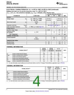
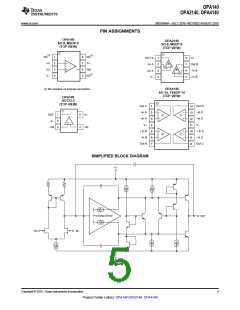
PACKAGE INFORMATION(1)
PRODUCT
PACKAGE-LEAD
PACKAGE DESIGNATOR
PACKAGE MARKING
OPA140
140
SO-8
D
DGK
DBV
D
OPA140
MSOP-8
SOT23-5
SO-8
O140
O2140A
2140
OPA2140
OPA4140
MSOP-8
TSSOP-14
SO-14
DGK
PW
D
O4140A
O4140A
(1) For the most current package and ordering information see the Package Option Addendum at the end of this document, or visit the
device product folder at www.ti.com.
2
Copyright © 2010, Texas Instruments Incorporated
Product Folder Link(s): OPA140 OPA2140 OPA4140

 TI [ TEXAS INSTRUMENTS ]