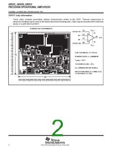
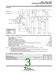
OP07C, OP07D, OP07Y
PRECISION OPERATIONAL AMPLIFIERS
SLOS099B – OCTOBER 1983 – REVISED AUGUST 1996
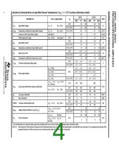
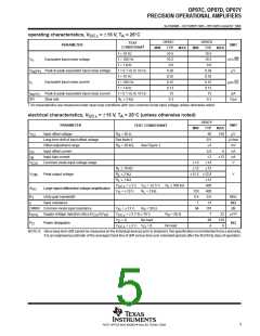
operating characteristics, V
= ±15 V, T = 25°C
CC
A
±
OP07C
TYP
10.5
10.2
9.8
OP07D
TYP
10.5
10.3
9.8
TEST
CONDITIONS
PARAMETER
UNIT
†
MIN
MAX
MIN
MAX
f = 10 Hz
f = 100 Hz
f = 1 kHz
V
V
I
Equivalent input noise voltage
nV/√Hz
µV
n
Peak-to-peak equivalent input noise voltage
Equivalent input noise current
f = 0.1 Hz to 10 Hz
f = 10 Hz
0.38
0.35
0.15
0.13
15
0.38
0.35
0.15
0.13
15
N(PP)
f = 100 Hz
pA/√Hz
n
f = 1 kHz
I
Peak-to-peak equivalent input noise current
Slew rate
f = 0.1 Hz to 10 Hz
pA
N(PP)
SR
R
≥ 2 kΩ
0.3
0.3
V/µs
L
†
All characteristics are measured under open-loop conditions with zero common-mode input voltage unless otherwise noted.
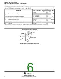
electrical characteristics, V
= ±15 V, T = 25°C (unless otherwise noted)
CC
A
±
OP07Y
TYP
60
†
PARAMETER
UNIT
TEST CONDITIONS
MIN
MAX
V
Input offset voltage
R
= 50 Ω
S
150
µV
µV/mo
mV
nA
IO
Long-term drift of input offset voltage
Offset adjustment range
See Note 6
0.5
R
= 20 kΩ,
See Figure 1
±4
S
I
I
Input offset current
0.8
6
IO
Input bias current
±2
±12
nA
IB
V
Common-mode input voltage range
±13
±12
±14
±13
V
ICR
OM
R
R
R
≤ 10 kΩ
≤ 2 kΩ
≤ 1 kΩ
L
L
L
V
Peak output voltage
±11.5 ±12.8
V
±12
V
= ±3 V,
V
= ±0.5 V,
= 2 kΩ
R
R
≤ 500 kΩ
400
CC±
O
L
A
Large-signal differential voltage amplification
VD
V
O
= ±10 V,
R
120
0.4
7
400
0.6
31
110
7
L
B
1
Unity-gain bandwidth
Input resistance
MHz
MΩ
r
i
CMRR Common-mode input resistance
V
V
V
V
= ±13 V,
R
= 50 Ω
94
dB
IC
S
k
Supply-voltage rejection ratio (∆V /∆V
)
= ±3 V to ±18 V,
= 50 Ω
32
150
8
µV/V
SVS
CC
IO
CC±
O
S
= 0,
No load
= 0,
80
4
P
D
Power dissipation
MΩ
= ±3 V,
V
O
No load
CC±
NOTE 6: Since long-term drift cannot be measured on the individual devices prior to shipment, this specification is not intended to be a warranty.
It is an engineering estimate of the averaged trend line of drift versus time over extended periods after the first thirty days of operation.
5
POST OFFICE BOX 655303 • DALLAS, TEXAS 75265

 TI [ TEXAS INSTRUMENTS ]