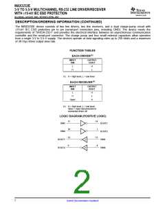
MAX3232E
3-V TO 5.5-V MULTICHANNEL RS-232 LINE DRIVER/RECEIVER
WITH ±15-kV IEC ESD PROTECTION
www.ti.com
SLLS664A–AUGUST 2005–REVISED APRIL 2007
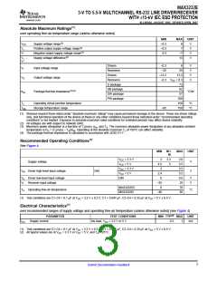
Absolute Maximum Ratings(1)
over operating free-air temperature range (unless otherwise noted)
MIN
–0.3
–0.3
0.3
MAX
6
UNIT
VCC
V+
Supply voltage range(2)
V
V
V
V
Positive output supply voltage range(2)
Negative output supply voltage range(2)
Supply voltage difference(2)
7
V–
–7
13
V+
–
V–
Drivers
–0.3
–25
6
25
V
V
V
V
VI
Input voltage range
Output voltage range
Receivers
Drivers
–13.2
13.2
VO
Receivers
D package
DB package
DW package
PW package
–0.3 VCC + 0.3
73
82
θJA
Package thermal impedance(3)(4)
°C/W
57
108
150
TJ
Operating virtual junction temperature
Storage temperature range
°C
°C
Tstg
–65
150
(1) Stresses beyond those listed under "absolute maximum ratings" may cause permanent damage to the device. These are stress ratings
only, and functional operation of the device at these or any other conditions beyond those indicated under "recommended operating
conditions" is not implied. Exposure to absolute-maximum-rated conditions for extended periods may affect device reliability.
(2) All voltages are with respect to network GND.
(3) Maximum power dissipation is a function of TJ(max), θJA, and TA. The maximum allowable power dissipation at any allowable ambient
temperature is PD = (TJ(max) – TA)/θJA. Operating at the absolute maximum TJ of 150°C can affect reliability.
(4) The package thermal impedance is calculated in accordance with JESD 51-7.
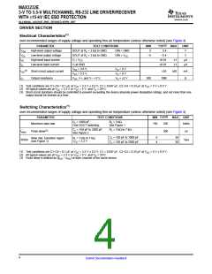
Recommended Operating Conditions(1)
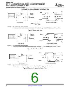
See Figure 4
MIN
NO
M
MAX
UNIT
VCC = 3.3 V
VCC = 5 V
VCC = 3.3 V
VCC = 5 V
DIN
3
4.5
2
3.3
5
3.6
5.5
5.5
5.5
0.8
25
Supply voltage
V
V
VIH Driver high-level input voltage
VIL Driver low-level input voltage
DIN
2.4
0
V
V
VI
Receiver input voltage
–25
0
MAX3232EC
MAX3232EI
70
TA Operating free-air temperature
°C
–40
85
(1) Test conditions are C1–C4 = 0.1 µF at VCC = 3.3 V ± 0.3 V; C1 = 0.047 µF, C2–C4 = 0.33 µF at VCC = 5 V ± 0.5 V.
Electrical Characteristics(1)
over recommended ranges of supply voltage and operating free-air temperature (unless otherwise noted) (see Figure 4)
PARAMETER
Supply current
TEST CONDITIONS
No load, VCC = 3.3 V or 5 V
MIN TYP(2) MAX
0.3
UNIT
ICC
1
mA
(1) Test conditions are C1–C4 = 0.1 µF at VCC = 3.3 V ± 0.3 V; C1 = 0.047 µF, C2–C4 = 0.33 µF at VCC = 5 V ± 0.5 V.
(2) All typical values are at VCC = 3.3 V or VCC = 5 V, and TA = 25°C.
3
Submit Documentation Feedback

 TI [ TEXAS INSTRUMENTS ]