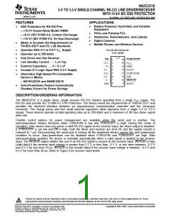
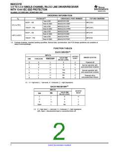
MAX3221E
3-V TO 5.5-V SINGLE-CHANNEL RS-232 LINE DRIVER/RECEIVER
WITH 15-kV IEC ESD PROTECTION
www.ti.com
SLLS686A–OCTOBER 2005–REVISED MAY 2006
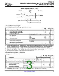
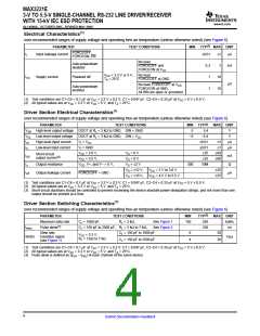
Electrical Characteristics(1)
over recommended ranges of supply voltage and operating free-air temperature (unless otherwise noted) (see Figure 6)
PARAMETER
FORCEOFF,
TEST CONDITIONS
MIN TYP(2) MAX UNIT
II
Input leakage current
±0.01
0.3
1
±1
µA
FORCEON, EN
No load,
FORCEOFF and
FORCEON at VCC
Auto-powerdown
disabled
1
mA
VCC = 3.3 V or 5 V, No load,
ICC
Supply current
Powered off
10
10
TA = 25°C
FORCEOFF at GND
µA
No load, FORCEOFF at VCC
FORCEON at GND,
All RIN are open or grounded
,
Auto-powerdown
enabled
1
(1) Test conditions are C1–C4 = 0.1 µF at VCC = 3.3 V ± 0.3 V; C1 = 0.047 µF, C2–C4 = 0.33 µF at VCC = 5 V ± 0.5 V.
(2) All typical values are at VCC = 3.3 V or VCC = 5 V, and TA = 25°C.
Driver Section Electrical Characteristics(1)
over recommended ranges of supply voltage and operating free-air temperature (unless otherwise noted) (see Figure 6)
PARAMETER
TEST CONDITIONS
MIN TYP(2)
MAX UNIT
VOH High-level output voltage DOUT at RL = 3 kΩ to GND, DIN = GND
5
5.4
–5.4
±0.01
±0.01
±35
V
V
VOL Low-level output voltage
DOUT at RL = 3 kΩ to GND, DIN = VCC
–5
IIH
IIL
High-level input current
Low-level input current
VI = VCC
±1
±1
µA
µA
VI = GND
VCC = 3.6 V,
VO = 0 V
±60
±60
Short-circuit
IOS
ro
mA
Ω
output current(3)
VCC = 5.5 V,
VO = 0 V
±35
Output resistance
VCC, V+, and V– = 0 V,
VO = ±2 V
VO = ±12 V,
VO = ±10 V,
300
10M
VCC = 3 V to 3.6 V
±25
±25
Ioff
Output leakage current
FORCEOFF = GND
µA
VCC = 4.5 V to 5.5 V
(1) Test conditions are C1–C4 = 0.1 µF at VCC = 3.3 V ± 0.3 V; C1 = 0.047 µF, C2–C4 = 0.33 µF at VCC = 5 V ± 0.5 V.
(2) All typical values are at VCC = 3.3 V or VCC = 5 V, and TA = 25°C.
(3) Short-circuit durations should be controlled to prevent exceeding the device absolute power-dissipation ratings, and not more than one
output should be shorted at a time.
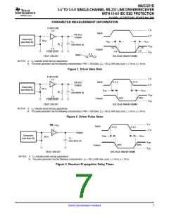
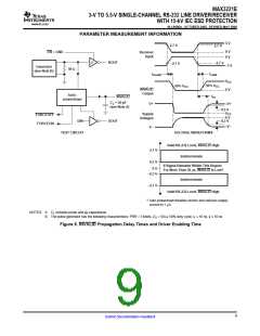
Driver Section Switching Characteristics(1)
over recommended ranges of supply voltage and operating free-air temperature (unless otherwise noted) (see Figure 6)
PARAMETER
TEST CONDITIONS
MIN
TYP(2)
250
MAX UNIT
Maximum data rate
Pulse skew(3)
CL = 1000 pF,
RL = 3 kΩ,
See Figure 1
See Figure 2
150
kbit/s
tsk(p)
CL = 150 pF to 2500 pF, RL = 3 kΩ to 7 kΩ,
100
ns
30
Slew rate,
transition region
(see Figure 1)
CL = 150 pF to 1000 pF
CL = 150 pF to 2500 pF
6
4
VCC = 3.3 V,
RL = 3 kΩ to 7 kΩ
SR(tr)
V/µs
30
(1) Test conditions are C1–C4 = 0.1 µF at VCC = 3.3 V ± 0.3 V; C1 = 0.047 µF, C2–C4 = 0.33 µF at VCC = 5 V ± 0.5 V.
(2) All typical values are at VCC = 3.3 V or VCC = 5 V, and TA = 25°C.
(3) Pulse skew is defined as |tPLH – tPHL| of each channel of the same device.
4
Submit Documentation Feedback

 TI [ TEXAS INSTRUMENTS ]