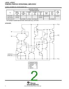
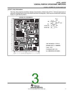
µA741, µA741Y
GENERAL-PURPOSE OPERATIONAL AMPLIFIERS
SLOS094A – NOVEMBER 1970 – REVISED JANUARY 1992
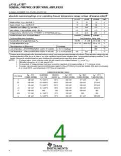
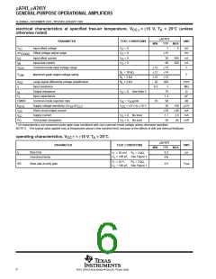
electrical characteristics at specified free-air temperature, V
otherwise noted)
= ±15 V, T = 25°C (unless
CC±
A
µA741Y
PARAMETER
TEST CONDITIONS
UNIT
MIN
TYP
1
MAX
V
Input offset voltage
V
O
V
O
V
O
V
O
= 0
= 0
= 0
= 0
6
mV
mV
nA
nA
V
IO
∆V
Offset voltage adjust range
Input offset current
±15
20
IO(adj)
I
I
200
500
IO
Input bias current
80
IB
V
Common-mode input voltage range
±12
±12
±10
20
±13
±14
±13
200
2
ICR
OM
R
R
R
= 10 kΩ
= 2 kΩ
≥ 2 kΩ
L
L
L
V
Maximum peak output voltage swing
V
A
VD
Large-signal differential voltage amplification
Input resistance
V/mV
MΩ
Ω
r
r
0.3
i
Output resistance
V
O
= 0, See Note 5
75
o
C
Input capacitance
1.4
90
pF
i
CMRR
Common-mode rejection ratio
V
V
= V
min
70
dB
IC
ICR
= ±9 V to ±15 V
k
Supply voltage sensitivity (∆V /∆V
)
30
150
±40
2.8
85
µV/V
mA
mA
mW
SVS
IO
CC
CC
I
I
Short-circuit output current
Supply current
±25
1.7
50
OS
V
V
= 0, No load
= 0, No load
CC
O
P
D
Total power dissipation
O
†
All characteristics are measured under open-loop conditions with zero common-mode voltage unless otherwise specified.
NOTE 5: This typical value applies only at frequencies above a few hundred hertz because of the effects of drift and thermal feedback.
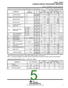
operating characteristics, V ± = ±15 V, T = 25°C
CC
A
µA741Y
TYP
0.3
PARAMETER
TEST CONDITIONS
= 20 mV, = 2 kΩ,
UNIT
MIN
MAX
t
r
Rise time
µs
V
C
R
L
I
L
= 100 pF, See Figure 1
Overshoot factor
5%
V
C
= 10 V,
= 100 pF, See Figure 1
R = 2 kΩ,
L
I
L
SR
Slew rate at unity gain
0.5
V/µs
6
POST OFFICE BOX 655303 • DALLAS, TEXAS 75265

 TI [ TEXAS INSTRUMENTS ]