SN74LVC07A
HEX BUFFERS/DRIVERS
WITH OPEN-DRAIN OUTPUTS
www.ti.com
SCAS595P–OCTOBER 1997–REVISED JANUARY 2007
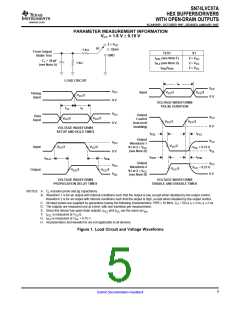
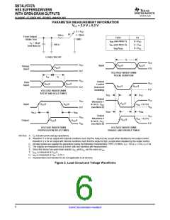
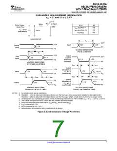
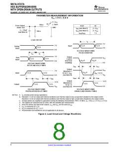
PARAMETER MEASUREMENT INFORMATION
VCC = 5 V ± 0.5 V
2 × V
CC
S1
Open
GND
500 Ω
From Output
Under Test
TEST
S1
2 × V
2 × V
t
(see Note F)
(see Note G)
PZL
CC
CC
C = 50 pF
(see Note A)
L
t
PLZ
500 Ω
t
/t
7 V
PHZ PZH
LOAD CIRCUIT
1.5 V
t
w
3 V
0 V
3 V
0 V
1.5 V
1.5 V
Input
Timing
Input
VOLTAGE WAVEFORMS
PULSE DURATION
t
su
t
h
3 V
0 V
Output
Control
(low-level
enabling)
Data
Input
V
CC
1.5 V
1.5 V
V /2
CC
V /2
CC
0 V
VOLTAGE WAVEFORMS
SETUP AND HOLD TIMES
t
t
PLZ
PZL
Output
Waveform 1
V
V
CC
3 V
0 V
V /2
CC
Input
1.5 V
1.5 V
S1 at 2 × V
V
OL
+ 0.3 V
CC
(see Note B)
OL
t
t
PHZ
PZH
t
t
PHL
PLH
Output
Waveform 2
S1 at 7 V
3.5 V
0 V
3.5 V
3.2 V
1.5 V
Output
1.5 V
1.5 V
V
OL
(see Note B)
VOLTAGE WAVEFORMS
PROPAGATION DELAY TIMES
VOLTAGE WAVEFORMS
ENABLE AND DISABLE TIMES
NOTES: A. C includes probe and jig capacitance.
L
B. Waveform 1 is for an output with internal conditions such that the output is low, except when disabled by the output control.
Waveform 2 is for an output with internal conditions such that the output is high, except when disabled by the output control.
C. All input pulses are supplied by generators having the following characteristics: PRR ≤ 10 MHz, Z = 50 Ω, t ≤ 2.5 ns, t ≤ 2.5 ns.
O
r
f
D. The outputs are measured one at a time, with one transition per measurement.
E. Since this device has open-drain outputs, t and t are the same as t
.
pd
PLZ
PZL
F.
G.
t
t
is measured at V /2.
CC
is measured at V + 0.3 V.
OL
PZL
PLZ
H. All parameters and waveforms are not applicable to all devices.
Figure 4. Load Circuit and Voltage Waveforms
8
Submit Documentation Feedback

 TI [ TEXAS INSTRUMENTS ]